
Printed Circuit Board Assembly (PCBA) is a basic viewpoint of advanced gadgets manufacturing, where components are collected onto a PCB to make utilitarian electronic gadgets. Over the past few decades, the complexity of PCBs has expanded essentially, driving to modern challenges in the manufacturing handle. Cutting edge electronic gadgets request littler, more complex plans, higher usefulness, and predominant execution, requiring more modern testing forms amid PCBA manufacturing.
The handle of PCBA includes numerous stages, counting plan, component determination, situation, patching, and testing. Of these, testing is significant as it makes a difference distinguish surrenders that may have happened amid manufacturing. For complex PCBAs, the testing handle must account for complex plans, tall component thickness, multi-layered sheets, and the require for quick prototyping and time-to-market. This article explores the different challenges related with testing complex PCBAs, as well as potential arrangements to these challenges.
Increasing Complexity of PCBs
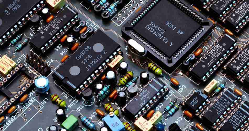
Miniaturization and Tall Component Density
One of the most noteworthy patterns in cutting edge hardware is the drive toward miniaturization. Gadgets are getting littler, however customers and businesses alike anticipate expanded usefulness. As a result, PCBs are planned with higher component thickness, which implies that more components are stuffed onto a single board. The challenge here is that as components get littler and more closely divided, the likelihood of manufacturing abandons increases.
Testing these thick sheets can be challenging, as conventional testing strategies like visual review or manual testing ended up less successful. The measure and nearness of components make it troublesome to physically get to person parts of the board. This requires progressed testing strategies such as Automated Optical Inspection (AOI) or X-ray assessment to distinguish issues without coordinate physical contact.
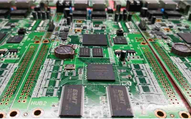
Multi-layered PCBs
In expansion to miniaturization, numerous advanced PCBs include different layers. Multi-layered PCBs permit for more complex circuitry and empower higher usefulness inside a littler impression. Be that as it may, the included complexity presents critical challenges in the testing stage. With multi-layered sheets, it’s harder to get to and assess inner layers for abandons, requiring more advanced non-invasive testing methods.
Complex Network and Functionality
In complex PCB congregations, the assortment of components and them interconnects increment exponentially. Components such as chip, memory chips, control controllers, and different sensors require to communicate successfully. Confirming that these components work together as aiming is one of the fundamental challenges in the utilitarian testing stage of PCBA. It is fundamental to guarantee that signals are accurately transmitted over the board, and any issues related to flag astuteness, electromagnetic Interference (EMI), or warm administration are tended to amid testing.
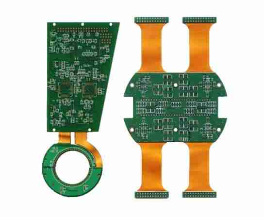
Flex PCBs and Rigid-Flex Designs
In a few applications, such as smart phones, therapeutic gadgets, or aviation components, flexible PCBs (Flex PCBs) or rigid-flex plans are utilized to meet the require for lightweight, bendable, and exceedingly tough circuit sheets. These plans posture special testing challenges due to their physical characteristics. Flex circuits can twist and turn, making it troublesome to hold them in put amid tests, and their non-standard shapes frequently require custom testing fixtures.
Types of Tests in PCBA Manufacturing
To handle the challenges related with complex PCBs, producers utilize a combination of testing strategies to guarantee the last item meets quality and unwavering quality measures. These include:
1. In-Circuit Test (ICT)
In-Circuit Testing (ICT) is one of the most commonly utilized testing strategies in PCBA manufacturing. It includes putting tests at particular test focuses on the board to check for coherence, resistance, capacitance, and other electrical parameters. ICT is exceedingly compelling for recognizing component-level absconds, such as open circuits, brief circuits, and inaccurate component placement.
However, ICT gets to be challenging for complex PCBs due to the need of available test focuses. As sheets gotten to be more thickly stuffed and multi-layered, the number of accessible test focuses diminishes, lessening the adequacy of conventional ICT systems.

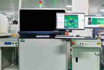
2. Automated Optical Inspection (AOI)
AOI employments cameras to capture high-resolution pictures of the PCB and recognize absconds such as lost components, patching blunders, or lost parts. AOI is a non-contact testing strategy that is well-suited for high-density and complex PCBAs, as it doesn’t require physical get to the board.
While AOI is compelling for recognizing surface-level surrenders, it battles to recognize issues in inner layers or patch joints covered up underneath components, such as ball grid arrays (BGAs). As PCBs gotten to be more complex, AOI alone may not give adequate scope for recognizing all potential defects.
3. X-Ray Inspection
X-ray assessment is a non-destructive testing strategy that permits producers to look at inside layers of the PCB and components. It is especially valuable for identifying covered up patch joint surrenders, such as those found in BGAs or other surface-mount devices (SMDs). X-ray review can too recognize issues like voids in patch joints, misaligned components, or inadequately patch coverage.
The challenge with X-ray assessment is its fetched and the mastery required to translate the comes about. Whereas it gives profitable understanding into hard-to-detect absconds, actualizing X-ray testing as a schedule step in the manufacturing prepare may not be doable for all producers due to the tall forthright costs of the equipment.

4. Functional Testing
Functional testing includes running the amassed PCB in a recreated working environment to confirm that it capacities accurately. This sort of test checks whether the board’s different components work together as anticipated beneath real-world conditions. Useful testing is especially imperative for complex PCBAs with progressed chip, sensors, and communication interfaces.
The challenge with useful testing lies in its setup. Making a practical test environment for complex gadgets can be time-consuming and expensive. Moreover, investigating utilitarian issues can be troublesome, as the source of the issue may not continuously be self-evident, requiring broad troubleshooting.
5. Boundary Filter Testing
Boundary filter testing, based on the IEEE 1149.1 standard, permits for testing the usefulness of person components and them interconnects without the required for physical test focuses. It is especially valuable for testing profoundly complex sheets where physical get to is limited.
While boundary filter testing can distinguish numerous sorts of abandons, it is restricted to components that bolster the boundary filter standard. Not all gadgets are congruous, and coordination boundary check into the plan stage may require extra assets and planning.
Common Manufacturing Defects in Complex PCBAs
1. Open Circuits
Open circuits happen when there is a break in the electrical pathway, anticipating current from streaming. This can result from destitute patching, broken follows, or component misalignment. Identifying open circuits gets to be more troublesome in multi-layered sheets where the imperfection may happen in an inside layer, making visual assessment ineffective.
2. Brief Circuits
Short circuits happen when two unintended electrical ways come into contact, causing over the top current to stream through the circuit. This can lead to overheating, component disappointment, or indeed harm to the whole board. In complex PCBs, the tall component thickness increments the probability of brief circuits, as little patching blunders or plan imperfections can make unintended connections.
3. Cold Patch Joints
Cold patch joints happen when the patch does not completely dissolve amid the patching handle, coming about in a frail association. These abandons are frequently troublesome to identify through visual review, as they may show up intaglio but fall flat beneath operational stretch. Cold patch joints are more likely to happen in complex PCBs with fine-pitch components or BGAs, where accomplishing appropriate patch scope is challenging.
4. Component Misplacement
In profoundly complex congregations, the chance of putting components in the off-base area increments, particularly when managing with little, similar-looking parts. Computerized situation machines can once in a while lose components due to blunders in the programming or mechanical glitches. Lost components can cause useful disappointments and may be troublesome to identify without progressed assessment methods like AOI.
5. Solder Bridges
A patch bridge happens when abundance patch makes an unintended association between two adjoining components or cushions. This is a common issue in high-density PCBs where the dispersing between components is negligible. Patch bridges can lead to brief circuits and are regularly troublesome to identify in thickly populated ranges of the board.
Test Challenges for Progressed PCBA Technologies
1. Ball Grid Arrays (BGAs)
BGAs are broadly utilized in advanced gadgets due to their capacity to give a huge number of I/O associations in a little impression. In any case, BGAs show critical challenges amid testing since their patch joints are found underneath the component, making them blocked off for visual review or conventional testing methods.
X-ray review is the most compelling way to identify surrenders in BGA solder joints, but it is costly and requires specialized gear. Also, revamping an inadequate BGA is troublesome due to its compact nature, making it basic to identify surrenders early in the manufacturing process.
2. Surface-Mount Devices (SMDs)
Surface-mount technology (SMT) permits components to be put specifically onto the surface of the PCB without the required for through-hole leads. Whereas SMT empowers more compact and effective plans, it presents challenges in terms of patching and testing.
SMDs frequently have fine-pitch leads that require exact fastening to dodge surrenders such as patch bridges or inadequately patch scope. Conventional testing strategies, like ICT, may not be appropriate for fine-pitch components, requiring the utilize of AOI, X-ray, or other non-contact review methods.
3. High-Frequency and High-Speed Circuits
As PCBs are utilized in more progressed applications, such as broadcast communications, aviation, and car frameworks, they must back high-frequency and high-speed signals. Guaranteeing flag astuteness in these applications is a major challenge, as indeed little abandons or format issues can lead to flag debasement or interference.
Testing high-frequency circuits requires specialized hardware and mastery to degree parameters such as impedance, flag reflection, and EMI. Furthermore, the complexity of high-speed circuits makes utilitarian testing more troublesome, as inconspicuous surrenders may as it was gotten to be clear beneath particular working conditions.
4. Thermal Management
Thermal management is another basic perspective of testing complex PCBAs, particularly in applications where tall control utilization produces critical warm. Components like control controllers, chip, and LEDs can create warm that must be disseminated to anticipate harm to the board.
Testing for warm execution includes guaranteeing that warm is appropriately overseen through the utilize of heatsinks, warm vias, and other cooling strategies. Warm imaging and infrared cameras are regularly utilized to distinguish hotspots on the board amid testing.
Solutions to Overcome Manufacturing Test Challenges
1. Design for Testability (DFT)
One of the most successful ways to address testing challenges in complex PCBAs is to consolidate Design for Testability (DFT) standards into the PCB plan stage. DFT includes planning the board with testing in intellect, guaranteeing that it has satisfactory test focuses, open components, and legitimate format for robotized inspection.
DFT can incorporate including test cushions for ICT, guaranteeing that basic signals are available for boundary check testing, and optimizing the format to minimize flag impedances. By planning the board with testing in intellect from the begin, producers can decrease the probability of surrenders and disentangle the testing process.
2. Automated Test Equipment (ATE)
Automated Test Equipment (ATE) is progressively utilized to test complex PCBAs, especially in high-volume manufacturing. ATE frameworks are competent of running numerous tests in parallel, giving comprehensive scope for electrical and useful parameters. ATE can too perform stretch testing, guaranteeing that the board capacities dependably beneath different natural conditions.
While ATE frameworks are costly, they can altogether diminish testing time and increment throughput, making them an appealing alternative for producers of complex PCBAs.
3. Advanced Imaging Techniques
To address the restrictions of conventional review strategies, producers can utilize progressed imaging strategies such as 3D AOI or 3D X-ray review. These strategies give a more point by point see of the board, permitting for the discovery of covered up absconds that may not be unmistakable in 2D imaging.
For case, 3D X-ray assessment can give cross-sectional pictures of the PCB, uncovering absconds in patch joints, inner layers, or components covered up underneath other parts. Whereas these strategies require specialized gear and ability, they offer prevalent imperfection discovery for complex PCBAs.
4. Continuous Monitoring and Real-Time Feedback
In complex PCB manufacturing, executing nonstop checking and real-time input frameworks can offer assistance recognize absconds as before long as they happen, lessening the time went through on revamp and manufacturing. By coordination sensors and information collection frameworks into the manufacturing line, producers can track key parameters such as temperature, fastening conditions, and situation exactness in real-time.
This real-time information can be utilized to alter the manufacturing handle on the fly, moving forward surrender and diminishing the number of flawed sheets that make it to the testing phase.
Conclusion
The manufacturing of complex PCBs presents various challenges, especially in the testing stage. As sheets ended up more complicated, with higher component thickness, numerous layers, and progressed functionalities, conventional testing strategies ended up less viable. To guarantee high-quality generation, producers must embrace progressed testing strategies such as AOI, X-ray review, and boundary check testing.
Incorporating Design for Testability (DFT) standards into the plan stage can essentially decrease the challenges related with testing complex PCBAs. Automated Test Equipment (ATE), progressed imaging strategies, and real-time input frameworks can advance upgrade the testing prepare, guaranteeing that absconds are recognized early and productively. By tending to these challenges, producers can move forward the unwavering quality and execution of their items whereas diminishing costs related with revamp and field disappointments.


