
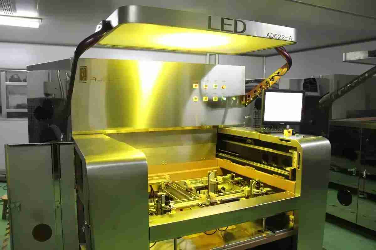
As an advanced quality inspection technology, AOI technology can comprehensively inspect components, welding, and mounting in SMT manufacturing.
AOI Main Applications
AOI is mainly used in solder paste printing inspection, component inspection, and after-welding assembly inspection.
1. Stencil Printing
AOI plays a significant role in the first step of the SMT printing process. In this stage, the AOI system can detect and verify the solder paste’s correctness, uniformity, and position.
Through high-resolution image acquisition, AOI can accurately identify excess or insufficient solder paste to ensure proper distribution on the PCB.
2. Component Placement
In the placement process, AOI is used to verify whether the SMT equipment has correctly placed all electronic components. It can detect the component’s position, orientation, and polarity to ensure that they meet the design drawings.
AOI can also identify potential printed circuit board assembly errors, such as offset, tilted, or missing components, to prevent these problems lead more serious quality issues in subsequent processes.

3. Reflow Soldering
During the welding process, the AOI system inspects the quality and connectivity of solder joints. It can detect whether the solder joints are excessive or insufficient and whether there are problems, such as cold solder joints, short circuits, or open circuits.

Through real-time image analysis, AOI can quickly identify unqualified welds and promptly notify operators to make PCB repairs to ensure the final welding quality.
4. Post-Solder Inspection
AOI still plays a role in the post-welding inspection process. It can detect defects in solder joints, the correctness of components, and possible circuit card assembly problems.
Through this step, the AOI system helps to screen out potential quality issues, ensuring that the product meets the required quality standards before entering the next circuit card manufacturing stage.
5. Final Inspection
Finally, AOI is used for comprehensive final inspection during the terminal detection stage of SMT.
It verifies component layout, solder joint connections, component correctness, and orientation of the circuit card.
The terminal inspection goal is to ensure the entire PCB meets the design specifications before final delivery. AOI achieves this goal through efficient automated inspection.
Advantages and Challenges of AOI
The wide application of AOI in various SMT processes brings many advantages, including:
Improve inspection efficiency: AOI can automatically and efficiently detect defects, saving manual inspection time.
Improve detection accuracy: AOI can use image recognition technology that can accurately detect subtle defects.
Reduce production costs: AOI can reduce the PCB rework rate and printed circuit board manufacturing costs.
However, AOI also faces some challenges, including:
High initial investment cost: Introducing an AOI system requires initial investment and subsequent maintenance, which increases circuit board manufacturer costs.
Cannot completely replace manual inspection: Although automated optical inspection systems can efficiently detect many problems,
But it still cannot replace some aspects of manual inspection, especially when dealing with complex defects.
Considering these advantages, PCB manufacturers can better utilize AOI technology to achieve a higher level of SMT manufacturing quality.


