
Development and Implementation of Flexible PCB, Proto PCB, PCB Board Industry
The world of electronics has changed dramatically in recent decades, and printed circuit boards (PCBs) play a key role in this transformation As technology advances at an unprecedented pace, sophisticated, compact electronics and it is a lot of work required for important innovations in PCB design and manufacturing Examines three important areas of modern PCB technology: flexible PCBs, prototype PCBs, and PCB board fabrication. We explore their unique characteristics, applications, and impact on businesses.
Flexible PCBs: Distorting some of the norms Related to Conventional Circuit Boards
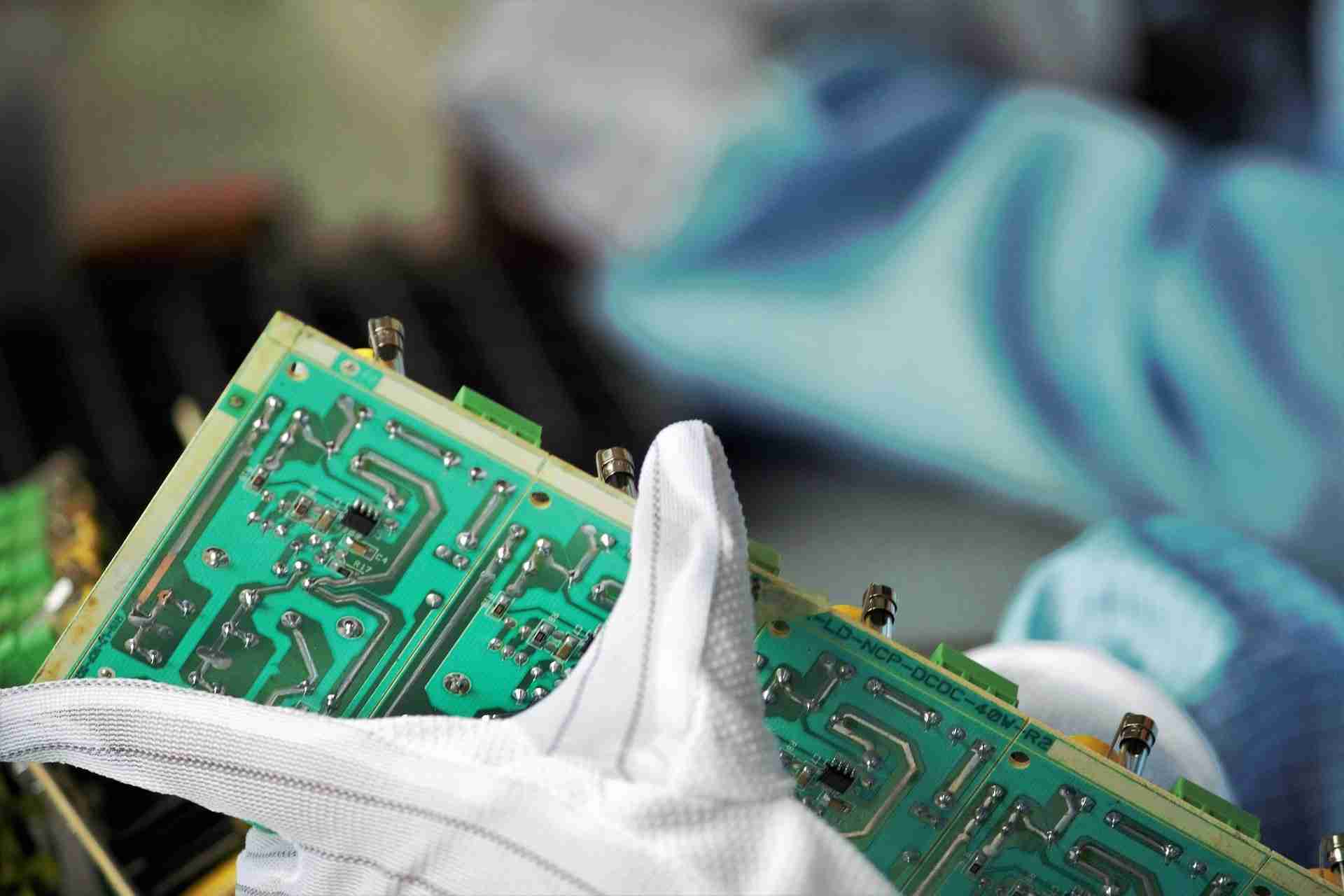
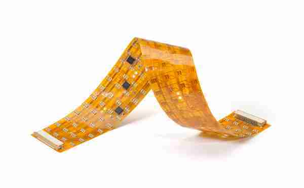
Flexible circuit boards (Flex PCBs) that are also known as flexible printed circuit boards can be regarded as the most revolutionary in the field of printed circuit boards manufacturing. In contrast to the rigid PCBs, these are made of similar support structures which comprise flexible substrate materials such as polyimide or polyester films and hence can be bent; folded and conformed into various shapes without hampering their electrical integrity to hold the damage.
Design and Construction
The core of a flexible PCB is basically a thin, transparent layer used to print or overwrite flowing errors. Typically, this substrate is made of materials such as polyimide with excellent thermal stability and chemical resistance. The conductive copper is usually copper, which can be utilized by various processes such as electrode position or lamination.
The process of manufacturing flex PCBs requires several steps:
1. Design and system architecture
2. Preparation of the substrate
3. Conductive Level Applications
4. Light resistance, coating and reflection
5. Engraving conductive patterns
6. To apply a coverlay or solder mask
7. Final inspection and testing
Advantages of flexible PCBs
1. Space savings: Flex PCBs can easily be bent or folded to any tight shape making it possible to develop compact devices.
2. Weight reduction: Due to their low volume they are used in portable electronics, computers and aerospace industries.
3. Dynamic flexibility: They can withstand repeated bending or bending periods, making them suitable for mechanical movements.
4. Improved reliability: Fewer connections are required, reducing potential points of failure.
5. Enhanced thermal management: The thin profile of the Flex PCB allows for better heat transfer.
6. 3D design capabilities: Flex PCBs enable creative three-dimensional circuit designs that are not possible with rigid boards.
Using flexible PCBs
The versatility of flex PCBs has led to their adoption in many industries: Due to high flexibility, flex PCBs have gained importance in many industries as discussed below.
1. Consumer electronics: Mobile phones, tablet and other wearable devices employ destructible and flexible storage system.
2. Vehicles: Flex PCBs are used in dashboard displays, control systems and sensors in all vehicles.
3. Medical devices: The ability to conform to different dimensions makes them ideal for implantable devices and diagnostic tools.
4. Space and Safety: The lightweight and reliable nature of the Flex PCB is important in satellite systems and flight instruments.
5. Industrial Equipment: Flex PCBs find utility in robotics, control systems, and sensors for harsh environmental monitoring.
Challenges and Future Developments
Though flex PCBs have a lot of advantages, they too are prone to some particular challenges. Material costs and process manufacturing costs, with respect to rigid PCBs, inherently go up. To make flex PCBs, inherent specialized knowledge is important for the process of designing that has to account for stress points and functionality when the board is bent or flexed.
Flex PCBs for the future will see more important improvements in durability, an increase in the number of layers that can be manufactured reliably, and development of newer materials with enhanced properties. Currently, research is being carried out on stretchable PCBs, which would also alter the face of wearable technology and medical implants.
Prototype PCBs: Bridging the Gap between Design and Production
A major step in electronic device development, prototype PCBs bridge the gap between concept design and full-scale production. They are useful for engineers and designers to test, refine, and validate their ideas prior to fully manufactured design concepts.
The significance of prototyping in the PCB development process lies in the following:
1. Verification of circuit design: Prototype PCB enables designers to test their circuit for its functionality in physical form.
2. Detection of errors: It is always better to find out a flaw in the design or a compatibility issue of a component at an initial stage, which consequently helps save time, money, and human resources in the long run.
3. Optimization: Through prototypes, both the layout and components can be “fine-tuned,” as well as the general performance of the PCB.
4. Cost estimation: Prototyping helps in the development of an accurate degree of cost that shall be required in the full production.
5. Investor presentations: Such functional prototypes, when presenting ideas to potential investors or stakeholders, could be very instrumental.
Types of Prototype PCBs
There are several ways to make a Prototype PCB with each having its own use cases and advantages. This includes:
1. Breadboard prototyping: This involves the use of solderless breadboards for easy assembly and testing of any circuit. It is not actually a real PCB but often used as the first step in most prototyping activities.
2. Perfboard prototyping: This involves soldering components onto a predrilled board with a grid of holes, making this method much more permanent than breadboarding. However, changes are still relatively easy to implement.
3. Etched prototypes: These are made using chemical etching processes, which can be performed at home or by small-scale professional services. They more closely resemble final PCBs but are usually restricted to a single or dual layer structure.
4. CNC-milled prototypes: Computer Numerical Control machines use eroding—fast milling away copper from a board—to generate single or double-sided PCB prototypes.
5. 3D-printed circuit boards: This technology is still under development, especially in prototyping PCBs for complex three-dimensional designs.
6. Professional prototyping services: Many of these PCB manufacturers offer rapid prototyping services with which small quantities of multi-layer PCBs of quality usually are produced in near-final product form.
Prototyping Process
Normally, the prototyping process follows these steps:
1. Schematic design: A detailed circuit diagram is obtained with the use of CAD software.
2. PCB layout: Translation of the schematic into a physical layout of a board, accounting for parameters like component placement and trace routing.
3. Design rule check: It checks that the design satisfies constraints imposed by the manufacturing process and electrical requirements.
4. Prototype fabrication: Actual fabrication of the physical PCB by any of the methods mentioned above.
5. Component assembly: Mounting of the required electronic components onto the board.
6. Testing and debugging: Checking that the prototype will actually do the job, and fixing any problems.
7. Iteration: The process of refining the design based on test results, and repeats until sufficient for purpose.
Advantages of Prototype PCBs
1. Risk mitigation: Problems identified and sorted out early reduces wallet-pinching mistakes in mass production.
2. Time-saving: Additional step in prototyping actually saves time because major redesigns at a later stage in the process are avoided.
3. Cost-effective: Prototyping investment offset generally through optimized designs and lesser production errors.
4. Better quality: Iterative prototyping leads to improved designs, hence a better quality end product.
5. Flexibility: Prototyping easily allows trying out various components, layout, and design.
Challenges in Prototype PCB Development
Despite the advantages that come with them, there are also challenges that distinctly associate with Prototype PCBs. These are:
1. Time factor: With rapid prototyping, sometimes this can be pretty hurried. This places pressure on the designer and the manufacturer for timely delivery of the product.
2. Cost considerations: although prototyping is much less expensive in regard to the big picture, it is still quite costly in regard to a multilayer design in micro amounts.
3. Functionality may be Limited: Prototypes might not practically epitomize the final product, either in terms of performance and durability.
4. Scaling Issues: There is a stage where what works successfully on a prototype cannot be flawlessly produced on a mass production environment.
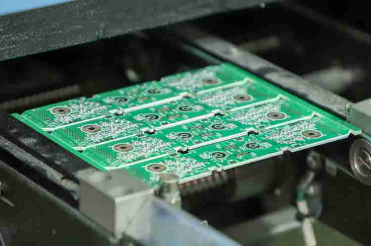
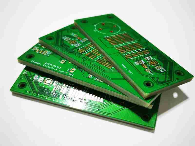
PCB Board Fabrication: The Art and Science of Bringing Designs to Life
PCB Board Making can be referred in other words as a process of manufacturing an actual printed circuit board whereby, a designer’s notion turns into a tangible product. Such a complicated process involves many steps and demands manufacturing in an advanced, technology-intensive, precise, and detailed way to establish the required quality of PCBs.
The PCB Fabrication Process
1. Design and File Preparation
The fabrication process starts with the PCB design files, normally in Gerber format. These files contain all information necessary for fabrication, including:
• Board outline and dimensions
• Copper layer layouts
• Solder mask and silkscreen details
• Drill locations and sizes
• Stack-up information for multi-layer boards
2. Material Selection
Choosing the right base material is crucial for the PCB’s performance. Common materials include:
• FR-4 (Flame Retardant 4): Glass reinforced epoxy laminate, common PCB.
– Polyimide — used in high-temperature applications and flex PCBs.
• Ceramic: Used in high frequency and high power.
• PTFE: Teflon is used in high-frequency microwaves.
3. Inner Layer Processing (for multi-layer PCBs)
• Copper-clad laminate is cleaned and covered with a photoresist.
• The circuit pattern is imaged onto the photoresist using UV light.
• Unexposed areas are removed, leaving the desired circuit pattern.
• Exposed copper is etched away, creating the inner layer circuits.
4. Layer Bonding
• Prepreg, or pre-impregnated bonding material, is used between layers in multilayer PCBs to keep inner layers one upon the other.
• The stack is pressed under high pressure and temperature to create a solid board.
5. Drilling
• Holes are drilled for component leads, vias, and mounting.
• Computer-controlled drilling machines ensure precise hole placement and size.
6. Copper Plating
• The entire board, including hole walls, is plated with a thin layer of copper.
• This process creates electrical connections between layers.
7. Outer Layer Imaging
• Similar to inner layer processing, the outer layers are imaged and etched to create the final circuit patterns.
8. Solder Mask Application
• A layer of solder mask, usually green in color but may be any other color, too, is applied to cover the copper traces from solder bridges during the assembly.
9. Surface Finish
Different finishes can be applied to protect the exposed copper and improve soldebility:
HASL: Hot Air Solder Leveling
ENIG: Electroless Nickel Immersion Gold
OSP: Organ Solderability Preservative
Immersion Tin or Silver
10. Silkscreen Printing
• Deposition of white epoxy ink legend for component designators, logos, and any desired marks on the board.
11. Electrical Testing
• Checking the continuity and isolation in the traces on the board.
12. Cutting and Profiling
• De-panel: To separate the individual PCBs from their panel and cut any slots or other special features shaped.
13. Final Inspection and Packaging
• Final boards are visually and functionally inspected before shipping.
Advanced Techniques of Fabrication
As the electronic world advances, so does the techniques of PCB fabrication:
1. HDI: The HDI technique uses microvias and fine line widths to increase the circuit density.
2. Embedded Components: The passive components such as resistors and capacitors may be fitted within the layers of the board, thus saving space and performance.
3. Rigid-Flex PCBs: Having rigid and flexible sections allowed together on a single board, greater three-dimensional designs can be achieved.
4. 3D Printed Electronics: This concept is just beginning; 3D printing sets out to develop custom PCB solutions having very odd geometries.
Challenges in PCB Fabrication
1. Miniaturization: As the devices keep on shrinking, PCBs need to adjust to small components and tighter tolerances.
2. High-Speed Design: Care in the fabrication of boards for high-frequency applications, with proper considerations for signal integrity and impedance control.
3. Environmental concerns: The PCB industry is working to develop more environmentally friendly manufacturing processes and materials.
4. Cost pressures: The eternal challenge—particularly in high-volume production—is maintaining the quality level at the best cost point.
5. Complex designs: Multilayer boards with mixed technologies—e.g., RF and digital circuits—require highly sophisticated manufacturing
processes.
Conclusion
The world of PCB innovation is one that continually changes with the persistent rate of alter driven through development in the hardware industry. Adaptable PCBs extend the conceivable outcomes of gadget plan, driving to littler and more flexible items for different businesses.
The proto PCBs proceed to play an critical part in creating that prepare since it permits a originator to substance out his or her thoughts and decrease dangers earlier to full-scale generation. In the interim, the creation strategies for the PCB board gotten to be progressively develop to meet the higher requests brought forward by the more complicated and miniaturized electronic devices.
New innovations ought to be presented, such as 3D printing and inserted components, which will alter the appearance of a PCB to unused conceivable outcomes of electronic plan and functionality.
By understanding adaptable PCBs in profundity, taking advantage of prototyping, and hence being upgraded on the most recent manufacture procedures, engineers and architects will be able to plan state-of-the-art gadgets that extend the limits of what is conceivable in the world of hardware.
Latest Blog


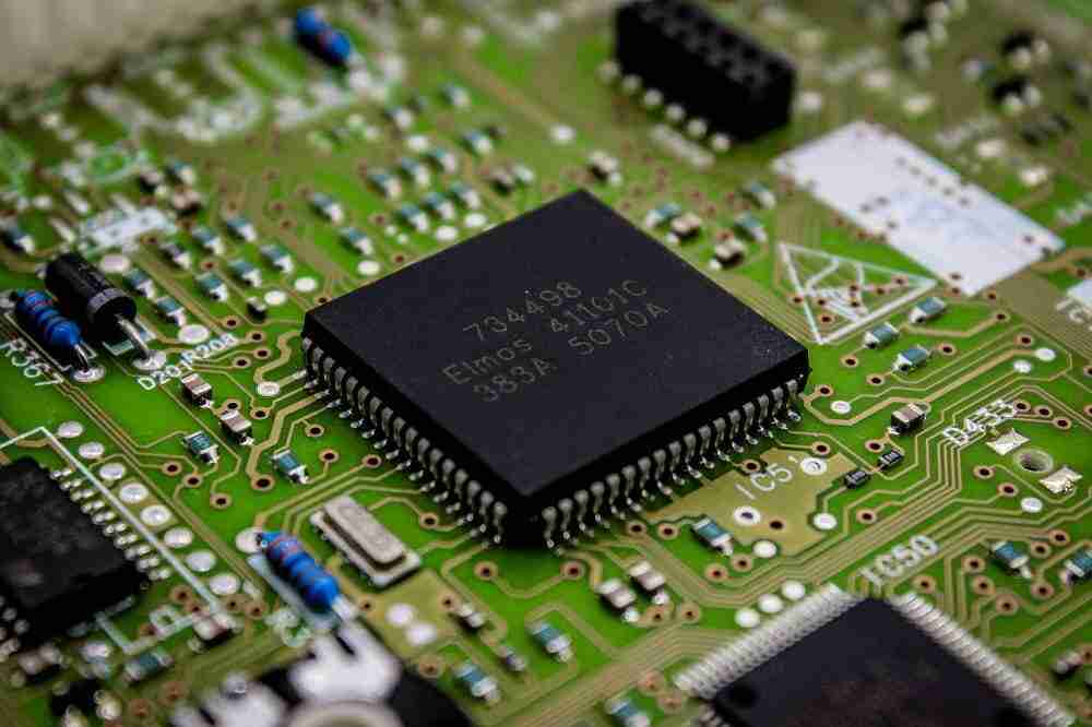
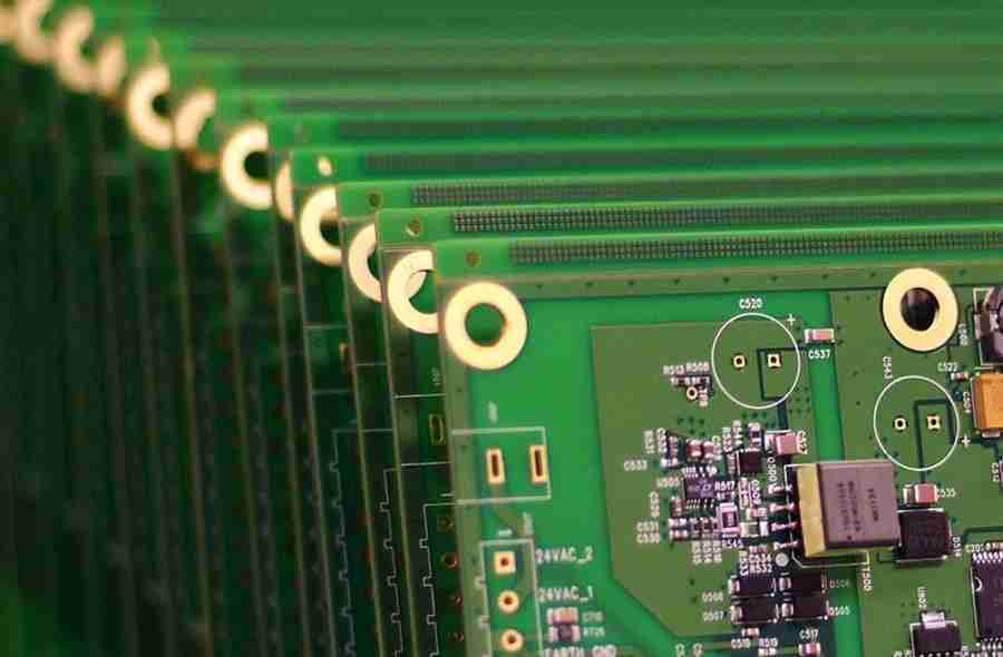
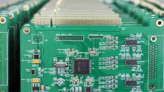
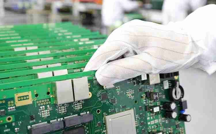

Table of Content
Contcat Us
Phone: +86-18123905375
Email: sales@circuitcardassembly.com
Skype: ali_youte
WhatsApp: +86-18123905375
Wechat: +86-18123905375

 Afrikaans
 Shqip
Shqip አማርኛ
አማርኛ العربية
 Հայերեն
 Azərbaycan dili
 Euskara
 Беларуская мова
 বাংলা
বাংলা Bosanski
 Български
 Català
 Cebuano
 Chichewa
 简体中文
简体中文 繁體中文
繁體中文 Corsu
Corsu Hrvatski
 Čeština
 Dansk
Dansk Nederlands
 Esperanto
 Eesti
Eesti Filipino
 Suomi
Suomi Français
 Frysk
Frysk Galego
 ქართული
 Deutsch
 Ελληνικά
 ગુજરાતી
 Kreyol ayisyen
 Harshen Hausa
 Ōlelo Hawaiʻi
 עִבְרִית
 हिन्दी
 Hmong
Hmong Magyar
 Íslenska
 Igbo
Igbo Bahasa Indonesia
 Gaeilge
 Italiano
 日本語
日本語 Basa Jawa
 ಕನ್ನಡ
ಕನ್ನಡ Қазақ тілі
 ភាសាខ្មែរ
 한국어
한국어 كوردی
كوردی Кыргызча
 ພາສາລາວ
 Latin
Latin Latviešu valoda
 Lietuvių kalba
 Lëtzebuergesch
 Македонски јазик
 Malagasy
 Bahasa Melayu
 മലയാളം
 Maltese
 Te Reo Māori
 मराठी
मराठी Монгол
 ဗမာစာ
ဗမာစာ नेपाली
 Norsk bokmål
 پښتو
پښتو فارسی
فارسی Polski
 Português
 ਪੰਜਾਬੀ
 Română
 Русский
 Samoan
 Gàidhlig
 Српски језик
 Sesotho
 Shona
Shona سنڌي
سنڌي සිංහල
සිංහල Slovenčina
 Slovenščina
 Afsoomaali
 Español
 Basa Sunda
 Kiswahili
 Svenska
 Тоҷикӣ
 தமிழ்
தமிழ் తెలుగు
 ไทย
ไทย Türkçe
 Українська
 اردو
اردو O‘zbekcha
 Tiếng Việt
 Cymraeg
 isiXhosa
 יידיש
יידיש Yorùbá
 Zulu
Zulu