
Embedded Components in PCBs: The Future of Compact Electronics
As the demand for smaller, more powerful, and productive electronic gadgets proceeds to surge, the conventional plan and format of printed circuit boards (PCBs) are being pushed to their limits. This expanding weight is fueling the require for inventive arrangements, and one of the most progressive concepts forming the future of compact hardware is the integration of embedded components in PCBs. By implanting inactive, dynamic, and indeed mechanical components straightforwardly into the PCB substrate, producers can create more compact, proficient, and vigorous devices.
In this detailed article, we’ll explore the world of embedded components in PCBs, how they work, their focal points, challenges, and their significant part in progressing the future of compact electronics.
What are Embedded Components in PCBs?
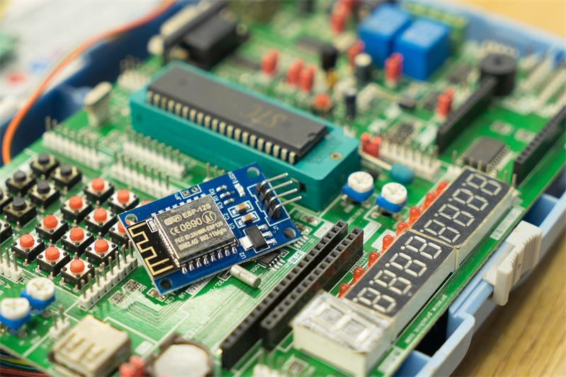
Embedded components are coordinates specifically into the layers of a PCB, as contradicted to being mounted on the surface. This incorporates both detached components like resistors, capacitors, and inductors, as well as dynamic components such as transistors, diodes, and integrated circuits (ICs).
The key qualification between conventional PCBs and those with embedded components is the vital arrangement of components inside the layers of the board. This permits for more compact plans and dispenses with the require for extra surface-mounted components (SMCs). Embedded components are set inside the inside structure of the PCB utilizing progressed manufacturing forms, which guarantee ideal electrical associations and integration with the rest of the circuit.

Types of Embedded Components
Embedded components in PCBs can by and large be classified into three primary types:
1. Passive Components: Resistors, capacitors, and inductors that direct current and voltage without opening up the signal.

2. Active Components: Gadgets such as transistors, diodes, and ICs that control and open up electrical signals.

3. Mechanical Components: These incorporate sensors or switches that may too be embedded to upgrade the usefulness of a device.
How Embedded Components Work
The prepare of inserting components inside a PCB includes putting detached or dynamic components interior the inward layers of the PCB amid the creation prepare. This is accomplished by either inserting discrete components or making the components through added substance manufacturing strategies such as thin-film testimony. The components are interconnected by the PCB’s electrical follows and vias, permitting for consistent communication between layers.
The process can be summarized in three key stages:
1. Design Stage: The format and positions of the implanted components are decided amid the plan stage. This incorporates bookkeeping for the estimate, warm dissemination, and the essential interconnects between the layers.
2. Manufacturing Stage: Amid the creation of the PCB, the implanted components are set interior the PCB stack-up some time recently the last cover handle. Lean layers of dielectric fabric and copper foils are squeezed together to shape a multi-layer PCB with the implanted components safely inside.
3. Testing and Confirmation: After manufacturing, thorough testing guarantees that all implanted components work accurately and are appropriately associated to the circuit.
Advantages of Embedded Components in PCBs
1. Compact and Space-Efficient Designs
One of the most critical focal points of inserting components is the capacity to make littler and more compact plans. By moving components from the surface to interior the PCB, originators can pack more usefulness into a littler impression. This is particularly vital in businesses such as customer hardware, where the request for compact gadgets like smartphones, wearables, and IoT gadgets is increasing.
2. Improved Signal Integrity
Embedded components offer prevalent flag astuteness due to diminished parasitic inductance and capacitance. Since the components are implanted inside the PCB and closer to the signals they oversee, flag ways are shorter, driving to lower resistance and less flag misfortunes. This is basic for high-speed advanced circuits and RF applications.
3. Upgraded Electrical Performance
With embedded components, the electrical execution of the PCB is upgraded. The near vicinity of the components to the substrate diminishes electromagnetic interference (EMI) and commotion. In expansion, warm dissemination is made strides, making it less demanding to oversee warm issues in thickly stuffed circuits.
4. Expanded Strength and Reliability
Embedded components are ensured inside the PCB layers, protecting them from outside natural components such as stickiness, tidy, and physical stretch. This expanded security comes about in a more tough and solid circuit, which is perfect for applications in cruel situations like aviation, car, and mechanical electronics.
5. Streamlined Manufacturing and Assembly
By coordination components inside the PCB, they require for surface-mounted devices (SMDs) is diminished, which rearranges the get together handle. Less components on the surface cruel less patch joints, driving to expanded unwavering quality and lower manufacturing costs. This moreover decreases the complexity of the bill of materials (BOM).
6. Taken a toll Investment funds in High-Volume Production
While the introductory taken a toll of creating implanted component innovation can be higher, it can lead to critical taken a toll investment funds in high-volume generation. By killing extra components and streamlining gathering, the by and large taken a toll of manufacturing huge amounts of PCBs can be reduced.
Applications of Embedded Components in PCBs
Embedded component innovation is revolutionizing different businesses, driving progressions in compact and high-performance hardware. Underneath are a few of the key applications:
1. Consumer Electronics

Consumer hardware, such as smart phones, tablets, wearables, and keen domestic gadgets, are quickly embracing embedded component innovation to meet the expanding request for littler, more capable, and energy-efficient gadgets. Implanting components inside the PCB permits producers to plan slenderer, lighter, and more feature-rich gadgets that offer improved usefulness and performance
2. Automotive Electronics
As vehicles ended up more zapped and independent, the request for compact, high-performance hardware is expanding. Implanted components can offer assistance diminish the measure and weight of car electronic frameworks whereas progressing unwavering quality in unforgiving working conditions.

3. Aerospace and Defense
The aviation and defense businesses require vigorous, solid gadgets that can withstand extraordinary situations. Embedded components offer progressed assurance and execution for mission-critical systems.
4. Medical Devices
Implantable restorative gadgets, such as pacemakers and hearing helps, advantage significantly from the miniaturization and unwavering quality advertised by embedded components. This innovation empowers the advancement of littler, more comfortable, and longer-lasting therapeutic devices.
5. IoT and Smart Devices
The expansion of IoT gadgets requires compact, low-power gadgets that can be effectively coordinates into an assortment of items and situations. Embedded components offer assistance accomplish these objectives whereas empowering expanded functionality.
6. High-Performance Computing
In information centers and supercomputers, where space and control proficiency are pivotal, embedded components can offer assistance make strides execution whereas decreasing the in general impression of computing systems.
Manufacturing Techniques for Embedded Components
Several manufacturing procedures have been created to empower the integration of implanted components in PCBs:
1. Laser Ablation
Laser removal is utilized to make exact cavities in the PCB layers where components can be put. This strategy permits for exact situating and measuring of embedded components.
2. Photoimageable Dielectrics
Photoimageable dielectric materials can be utilized to make cavities and structures inside the PCB layers. These materials can be specifically uncovered and created to frame the craved designs for implanting components.
3. Additive Manufacturing
Additive manufacturing strategies, such as 3D printing, are being investigated for making PCBs with embedded components. This approach permits for more noteworthy plan adaptability and the potential for customized, on-demand production.
4. Lamination Techniques
Advanced cover forms are utilized to bond numerous layers of the PCB together, typifying the embedded components inside the structure.
5. Direct Compose Technologies
Direct compose innovations, such as inkjet printing and vaporized fly printing, are being created to straightforwardly store conductive follows and indeed a few detached components onto the PCB substrate.
Future Patterns and Innovations
As implanted component innovation proceeds to advance, a few patterns and developments are emerging:
1. 3D Printed Electronics

The combination of implanted components and 3D printing innovations is opening up unused conceivable outcomes for making complex, three-dimensional electronic structures. This seem lead to totally unused frame components and applications for electronic devices.
2. Flexible and Stretchable Electronics
Embedding components in adaptable substrates is empowering the advancement of bendable and stretchable gadgets. This innovation has applications in wearable gadgets, delicate mechanical autonomy, and similar sensors.

3. Integration with Progressed Materials
Researchers are investigating the integration of embedded components with progressed materials such as graphene and other 2D materials. This seem lead to critical changes in execution and functionality.
4. Embedded Antennas
Embedding radio wires specifically into PCBs can make strides the execution and decrease the estimate of remote gadgets. This is especially imperative for 5G and IoT applications.
5. Power Hardware Integration
Embedding control components such as inductors and transformers is getting to be more common, empowering more compact and productive control supply designs.
6. Artificial Insights and Machine Learning

As AI and machine learning gotten to be more predominant in electronic gadgets, embedded components will play a pivotal part in empowering more capable and productive edge computing capabilities.
Challenges for the Future
While the future of embedded components in PCBs looks promising, there are still a few challenges that require to be addressed:
1. Design Devices and Software
More progressed plan apparatuses and computer program are required to completely use the potential of embedded components. These instruments ought to be able to handle the complexity of 3D plan and recreate the execution of implanted frameworks accurately.
2. Materials Research
Continued investigate into unused materials is fundamental to move forward the execution, unwavering quality, and manufacturability of embedded components. This incorporates creating way better dielectric materials, conductive materials, and encapsulants.
3. Manufacturing Scalability
As request for implanted component innovation develops, manufacturing forms require to gotten to be more versatile and cost-effective. This may require critical ventures in unused gear and processes.
4. Education and Training
The hardware industry will require to contribute in instruction and preparing to create the abilities required for planning and manufacturing PCBs with implanted components.
5. Standardization Efforts
Industry-wide guidelines for embedded component plan, manufacturing, and testing require to be created to guarantee consistency and compatibility over diverse producers and suppliers.
Conclusion
Embedded components in PCBs speak to a noteworthy step forward in the advancement of electronic plan. By coordination components specifically into the PCB structure, architects can make littler, more proficient, and more solid electronic gadgets. This innovation is as of now making waves in businesses such as customer hardware, car, aviation, and restorative gadgets, and its affect is as it were anticipated to develop in the coming years.
As with any developing innovation, there are challenges to overcome, counting plan complexity, manufacturing forms, and standardization. Be that as it may, the potential benefits of implanted components distant exceed these impediments. The future of compact hardware lies in the proceeded advancement and refinement of implanted component technology.
As we see to the future, we can anticipate to see indeed more inventive applications of implanted components, from adaptable and stretchable gadgets to progressed 3D-printed structures. The integration of embedded components with other cutting-edge innovations such as fake insights, 5G communications, and progressed materials will drive the following era of electronic devices.
For engineers, originators, and producers in the gadgets industry, remaining side by side of advancements in implanted component innovation will be vital. Those who can viably use this innovation will be well-positioned to make the imaginative, compact, and high-performance electronic gadgets that will shape our future.
In conclusion, embedded components in PCBs are not fair a passing drift but a crucial move in how we approach electronic plan. As the innovation proceeds to develop and advance, it will play a progressively imperative part in forming the future of compact gadgets, empowering modern conceivable outcomes and pushing the boundaries of what’s conceivable in electronic gadget plan.
Latest Blog


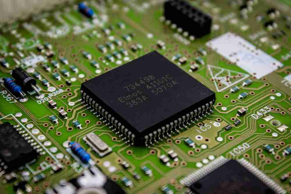
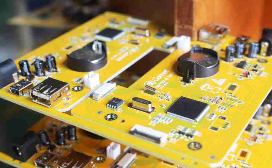

Table of Content
Contcat Us
Phone: +86-18123905375
Email: sales@circuitcardassembly.com
Skype: ali_youte
WhatsApp: +86-18123905375
Wechat: +86-18123905375

 Afrikaans
 Shqip
Shqip አማርኛ
አማርኛ العربية
 Հայերեն
 Azərbaycan dili
 Euskara
 Беларуская мова
 বাংলা
বাংলা Bosanski
 Български
 Català
 Cebuano
 Chichewa
 简体中文
简体中文 繁體中文
繁體中文 Corsu
Corsu Hrvatski
 Čeština
 Dansk
Dansk Nederlands
 Esperanto
 Eesti
Eesti Filipino
 Suomi
Suomi Français
 Frysk
Frysk Galego
 ქართული
 Deutsch
 Ελληνικά
 ગુજરાતી
 Kreyol ayisyen
 Harshen Hausa
 Ōlelo Hawaiʻi
 עִבְרִית
 हिन्दी
 Hmong
Hmong Magyar
 Íslenska
 Igbo
Igbo Bahasa Indonesia
 Gaeilge
 Italiano
 日本語
日本語 Basa Jawa
 ಕನ್ನಡ
ಕನ್ನಡ Қазақ тілі
 ភាសាខ្មែរ
 한국어
한국어 كوردی
كوردی Кыргызча
 ພາສາລາວ
 Latin
Latin Latviešu valoda
 Lietuvių kalba
 Lëtzebuergesch
 Македонски јазик
 Malagasy
 Bahasa Melayu
 മലയാളം
 Maltese
 Te Reo Māori
 मराठी
मराठी Монгол
 ဗမာစာ
ဗမာစာ नेपाली
 Norsk bokmål
 پښتو
پښتو فارسی
فارسی Polski
 Português
 ਪੰਜਾਬੀ
 Română
 Русский
 Samoan
 Gàidhlig
 Српски језик
 Sesotho
 Shona
Shona سنڌي
سنڌي සිංහල
සිංහල Slovenčina
 Slovenščina
 Afsoomaali
 Español
 Basa Sunda
 Kiswahili
 Svenska
 Тоҷикӣ
 தமிழ்
தமிழ் తెలుగు
 ไทย
ไทย Türkçe
 Українська
 اردو
اردو O‘zbekcha
 Tiếng Việt
 Cymraeg
 isiXhosa
 יידיש
יידיש Yorùbá
 Zulu
Zulu