
In the realm of advanced gadgets, Printed Circuit Boards (PCBs) serve as the establishment for essentially each electronic gadget we utilize nowadays. From smart phones and computers to mechanical hardware and medical devices, PCBs are the unsung heroes that empower the usefulness and miniaturization of electronic items. This article digs into the world of PCBs, investigating their sorts, manufacturing forms, assembly strategies, and the progressive affect of Printed Circuit Board Assembly (PCBA), Surface Mount Technology (SMT), Surface Mount PCB, and SMT PCB Boards, to get it their parts and importance in cutting edge electronics.

Printed Circuit Boards (PCBs) are the foundational building pieces of most electronic gadgets. They are the physical stage upon which electrical components, circuits, and frameworks are mounted and interconnected. These Boards have revolutionized the gadgets industry by empowering the miniaturization of gadgets and moving forward the proficiency of generation processes.
Understanding Printed Circuit Boards (PCBs)
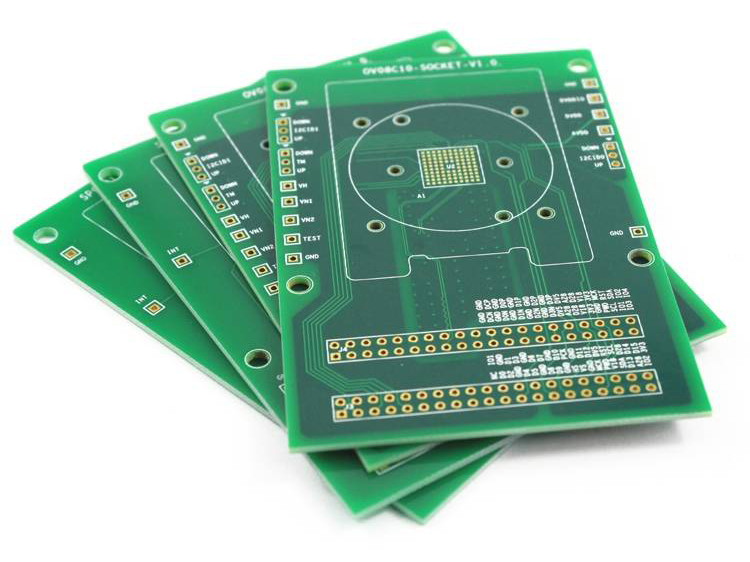
A Printed Circuit Board is a level board made of protection fabric, ordinarily fiberglass, with conductive pathways carved or printed onto its surface. These pathways, ordinarily made of copper, interface different electronic components such as resistors, capacitors, integated circuits, and connectors. PCBs give both mechanical bolster for the components and electrical associations between them, permitting for the creation of complex electronic circuits in a compact and dependable frame factor.

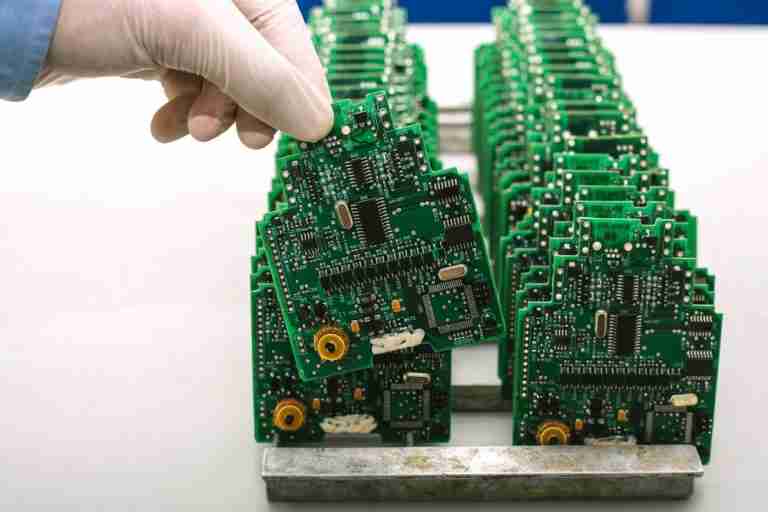
Printed Circuit Board Assembly, regularly shortened as PCBA, is the prepare of assembly the electronic components onto a uncovered PCB to shape a working circuit. This handle includes mounting different components, such as resistors, capacitors, coordinates circuits, and connectors, onto the board utilizing either Surface Mount Technology (SMT) or Through-Hole Technology (THT).

In substance, PCBA is the total organize of manufacturing where the electronic components are put, fastened, and tried to guarantee they perform as planning. The result is a completely operational circuit that can be coordinates into bigger systems.
Steps in the PCBA Process
1. Solder Glue Application: The to begin with step includes applying patch glue onto the PCB utilizing a stencil. Patch glue is a blend of little patch particles and flux, which makes a difference make a solid electrical and mechanical bond between the components and the PCB.

2. Component Situation: Once the patch glue is connected, electronic components are carefully put on the board utilizing a pick-and-place machine. This machine naturally places components with tall accuracy onto the fitting pads.

3. Reflow Fastening: After the components are put, the board is warmed in a reflow stove. The warm dissolves the patch glue, making strong patch joints between the components and the PCB.

4. Inspection and Testing: Once the reflow handle is total, the board experiences visual assessment or automatic optical inspection (AOI) to guarantee appropriate patch joints and component arrangement. Extra testing, such as in-circuit testing (ICT) or utilitarian testing, may be conducted to affirm that the circuit is working as expected.

5. Final Assembly: After all assessments and testing, the collected PCB may be coordinates into a last item or experience assist alterations, depending on the application.
Advantages of PCBA
• Cost Effectiveness: PCBA empowers the mass generation of electronic gadgets with steady quality, diminishing labor costs and expanding generation efficiency.
• High Unwavering quality: The utilize of computerized machines in the assembly prepare moves forward the unwavering quality of the last item by minimizing human error.
• Flexibility: PCBA is adaptable sufficient to oblige a wide extend of components, from basic resistors to complex microcontrollers, making it reasonable for different applications in distinctive industries.
Types of PCBs
1. Single-sided PCBs: These have conductive tracks on as it were one side of the board. They are straightforward and cost-effective but restricted in complexity.

2. Double-sided PCBs: Highlighting conductive tracks on both sides of the board, these offer more noteworthy circuit thickness and flexibility.
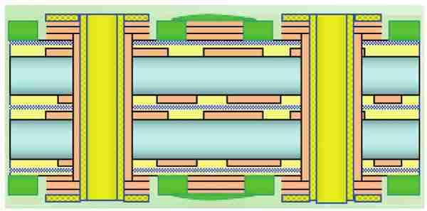
3. Multilayer PCBs: Comprising of three or more conductive layers, these Boards permit for exceedingly complex circuits in a compact space.
4. Rigid PCBs: Made from strong, unbendable materials, these are the most common sort of PCBs.
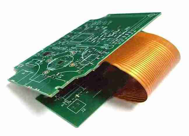
5. Flexible PCBs: Built utilizing adaptable materials like polyimide, these Boards can twist and crease, permitting for interesting shape variables and applications.
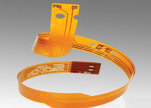
6. Rigid-flex PCBs: A combination of inflexible and adaptable board innovations, advertising the best of both universes for certain applications.
PCB Manufacturing Process
The generation of PCBs includes a few perplexing steps:
1. Design: Engineers make the circuit format utilizing Computer-Aided Design (CAD) software.
2. Printing: The plan is printed onto the copper-clad board utilizing photoresist.
3. Etching: Undesirable copper is evacuated, taking off as it were the wanted conductive pathways.
4. Drilling: Gaps are penetrated for component leads and vias (associations between layers).
5. Plating: Copper is electroplated onto the board to make through-holes and vias.
6. Solder cover application: A lean layer of polymer is connected to ensure the copper traces.
7. Silkscreen printing: Component designators and other markings are printed on the board.
8. Final testing: The uncovered PCB is tried for progression and shorts.
PCB Assembly(PCBA)
Once the uncovered PCB is made, it needs to be populated with components to make a useful electronic circuit. This handle is known as PCB Assembly(PCBA). There are two fundamental strategies of PCBA:
1. Through-Hole Technology (THT)

In THT, component leads are embedded through gaps in the PCB and fastened on the inverse side. This strategy offers solid mechanical bonds and is still utilized for components that require to withstand mechanical push or tall control. In any case, it has impediments in terms of miniaturization and automation.
2. Surface Mount Technology (SMT)
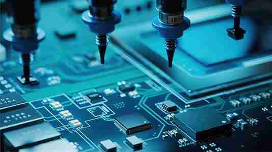
SMT has revolutionized the gadgets industry by permitting components to be mounted specifically onto the surface of the PCB. This strategy offers various focal points over THT, including:
• Increased component density
• Smaller by and large measure of the wrapped up product
• Improved electrical execution due to shorter lead lengths
• Better appropriateness for computerized assembly
• Lower generation costs at tall volumes
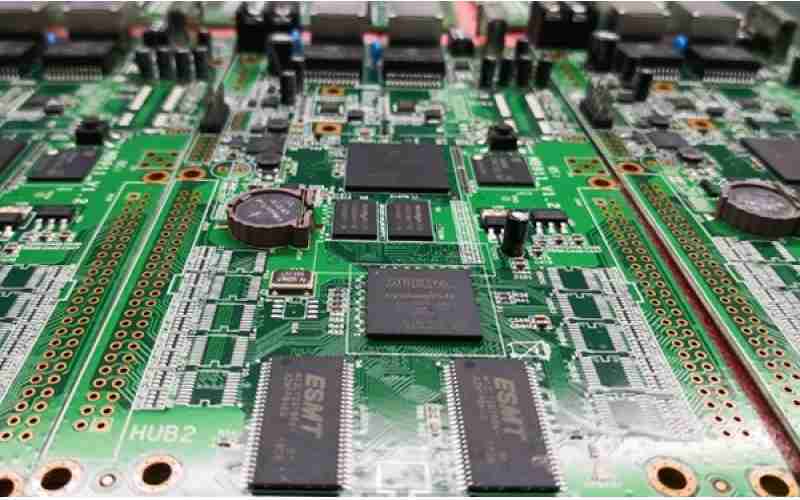
SMT Circuit Boards and Components
SMT circuit Boards are particularly planned to suit surface mount components. These components, known as Surface Mount Gadgets (SMDs), are much littler than their through-hole partners and have either little metal tabs or balls of patch for associations instep of wire leads.
Common sorts of SMD components include:
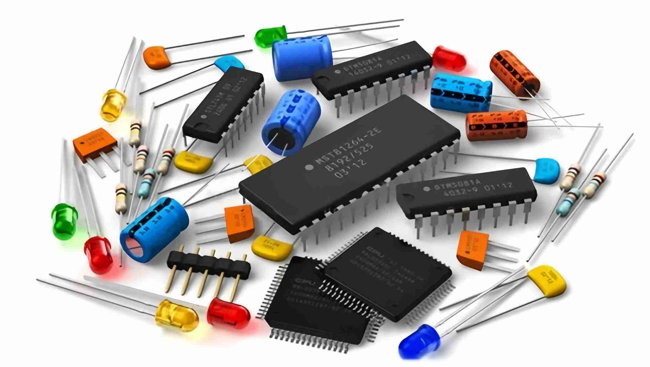
• Resistors and capacitors in chip packages
• Integrated circuits in different bundle sorts (e.g., SOT, QFP, BGA)
• LEDs and other optoelectronic devices
• Inductors and transformers
• Connectors and switches
SMT PCB Assembly Process
The SMT assembly prepare regularly includes the taking after steps:
1. Solder Glue Application: A stencil is utilized to apply patch glue to the fitting cushions on the PCB.
2. Component Situation: Pick-and-place machines precisely position SMD components onto the patch paste.
3. Reflow Patching: The board is warmed in a reflow stove, softening the patch glue and making changeless connections.
4. Inspection: Automated optical inspection (AOI) or X-ray assessment frameworks check for defects.
5. Testing: Useful and in-circuit tests guarantee the collected board works as intended.
For Boards that require both SMT and THT components, the SMT components are more often than not amassed to begin with, taken after by the through-hole components in a isolated process.
Advantages of SMT PCB Boards
1. Miniaturization: SMT permits for much higher component thickness, empowering the creation of littler, lighter electronic devices.
2. Improved Execution: Shorter association ways diminish parasitic capacitance and inductance, progressing high-frequency performance.
3. Increased Unwavering quality: Less bored gaps and shorter leads result in less potential focuses of failure.
4. Cost-Effectiveness: Whereas introductory setup costs may be higher, SMT is more cost-effective for high-volume generation due to expanded robotization and diminished fabric costs.
5. Double-Sided Assembly: SMT components can be set on both sides of the PCB, encourage expanding circuit density.
6. Improved Stun and Vibration Resistance: The lower mass of SMD components makes them less vulnerable to mechanical stresses.
Challenges in SMT PCB Assembly
Despite its numerous points of interest, SMT PCB Assembly too presents a few challenges:
1. Heat Affectability: A few components may be harmed by the tall temperatures utilized in reflow soldering.
2. Difficulty in Manual Revamp: The little measure of SMD components makes manual repairs more challenging.
3. Thermal Administration: The tall component thickness can lead to warm dissemination issues in a few designs.
4. Solder Joint Unwavering quality: Legitimate plan and prepare control are significant to guarantee dependable patch joints, particularly for ball network cluster (BGA) components.
5. Equipment Costs: SMT assembly requires specialized and regularly costly gear, which can be a obstruction for small-scale production.
Advanced SMT Techniques
As hardware proceed to advance, modern SMT methods are being created to meet the requests of progressively complex and miniaturized designs:
1. Fine-Pitch Innovation: This includes working with components that have greatly near lead dividing, requiring progressed arrangement and patching techniques.
2. Chip-Scale Packaging (CSP): These bundles are about the same estimate as the silicon pass on they contain, pushing the limits of miniaturization.
3. 3D Bundle Stacking: Numerous chips are stacked vertically to increment usefulness whereas minimizing footprint.
4. Embedded Components: Inactive components are inserted inside the PCB layers, sparing indeed more space on the surface.
5. Wafer-Level Packaging (WLP): Components are bundled whereas still in wafer frame, coming about in amazingly little packages.
Quality Control in SMT PCB Assembly
Ensuring the quality and unwavering quality of SMT PCB assemblies is vital. Different review and testing strategies are employed:
1. Automated Optical Inspection (AOI): High-resolution cameras and picture handling program identify surrenders such as lost components, inaccurate introductions, and patch problems.
2. X-ray Review: Especially valuable for reviewing covered up patch joints in BGA and other complex packages.

3. In-Circuit Testing (ICT): Tests contact focuses on the PCB to test person components and connections.

4. Functional Testing: The gathered PCB is tried beneath working conditions to guarantee it performs as intended.
5. Environmental Push Screening: Boards are subjected to temperature cycling, vibration, and other stresses to distinguish potential weaknesses.
Environmental Considerations
The hardware industry is progressively centring on natural maintainability. This influences PCB and PCBA forms in a few ways:
1. Lead-Free Patching: Controls like RoHS have driven to the far reaching appropriation of lead-free patch, which requires distinctive prepare temperatures and can influence reliability.
2. Halogen-Free PCB Materials: These materials decrease natural affect but may have distinctive properties that influence manufacturing and performance.
3. Design for Recyclability: Contemplations are made in the plan stage to encourage less demanding reusing of electronic items at end-of-life.
4. Energy Effectiveness: Both in terms of the control utilization of the last item and the vitality utilized in the manufacturing process.
Future Patterns in PCB and SMT Technology
The field of PCB and SMT innovation proceeds to advance quickly. A few developing patterns include:
1. Additive Manufacturing: 3D printing innovations are being investigated for PCB generation, possibly permitting for more complex geometries and implanted components.
2. Flexible and Stretchable Hardware: Headways in materials and manufacturing procedures are empowering hardware that can twist, extend, and acclimate to different shapes.
3. Increased Computerization and AI: Machine learning calculations are being utilized to optimize component arrangement, foresee absconds, and progress generally manufacturing efficiency.
4. Higher Recurrence Applications: As 5G and other high-frequency applications ended up more predominant, PCB materials and plans are advancing to meet these challenges.
5. Integration with Other Innovations: PCBs are being coordinates with advances like MEMS (Micro-Electro-Mechanical Systems) and photonics, obscuring the lines between diverse areas of electronics.
Conclusion
Printed Circuit Boards, PCB Assembly, and Surface Mount Technology frame the spine of advanced gadgets. From the essential concept of a PCB to the progressed strategies of SMT, these advances have empowered the extraordinary miniaturization and usefulness of electronic gadgets we see nowadays. As we see to the future, proceeded progressions in materials, manufacturing forms, and plan strategies guarantee to thrust the boundaries of what’s conceivable in hardware indeed further.
Whether you’re a specialist working on a DIY extend or an design planning the another groundbreaking electronic item, understanding the essentials and most recent improvements in PCB and SMT technology is vital. As electronics continue to permeate every aspect of our lives, the importance of these technologies in shaping our technological landscape cannot be overstated.


