
How are PCB Electronic Boards Made? The Manufacturing Process Unveiled
In the world of electronics, the PCB Electronic Board plays a essential part in making electronic gadgets work as they ought to. Whether it’s a Smartphone, a computer, or indeed restorative electronics, PCB electronic boards serve as the spine that interfaces and permits diverse components to work together. But have you ever wondered how these boards are made? Understanding the PCB manufacturing handle can shed light on the complicated and nitty gritty steps that go into making these basic parts. This Content takes you through the handle, from plan to final assembly.
What is a PCB Electronic Board?
A PCB (Printed Circuit Board) is a level board that gives mechanical back and electrical associations for electronic components. The board is ordinarily made of non-conductive fabric, such as fiberglass, and has conductive pathways (as a rule copper) carved onto its surface to permit electrical signals to stream between diverse components like resistors, capacitors, and chips. PCBs can extend from straightforward single-layer boards to profoundly complex multi-layered frameworks utilized in progressed technology.
Step 1: Plan and Format of the PCB Electronic Board
The to begin with arrange of PCB electronic board manufacturing is plan and format. This is one of the most basic stages in the whole handle, as it decides how the board will work. Engineers utilize specialized PCB design software like Altium Creator, Hawk, or KiCad to make the schematic and format for the board.
The plan stage includes a few key steps:
1. Schematic Creation: Engineers start by making a schematic graph that diagrams the associations between different electronic components. This schematic appears how signals will stream over the board and where each component will be placed.
2. Layout Plan: After the schematic is total, the format stage starts. Amid this stage, engineers characterize the board’s measure, shape, and the area of components. They moreover characterize the copper follows (wires) that interface the components. The format too incorporates layer definition for multi-layer PCBs, where follows are directed between distinctive layers.
3. Design Rules Check (DRC): After the introductory format is total, a Plan Run the show Check is performed to guarantee there are no mistakes in the plan. This incorporates checking the dispersing between components, follows, and vias to make beyond any doubt the plan complies with manufacturing standards.
4. Gerber Records: Once the plan is approved, engineers produce Gerber records, which contain all the data almost the PCB format, counting follow designs, gap areas, and the situation of components. These records are sent to the producer to start the manufacture process.
Step 2: PCB Electronic Board Fabric Selection
The another step in the manufacturing prepare is choosing the suitable materials for the PCB electronic board. The essential materials utilized in PCB manufacturing are:
• Substrate: The substrate is the non-conductive base fabric of the board. Fiberglass (particularly, FR4) is the most commonly utilized substrate for general-purpose PCBs due to its quality, solidness, and cost-effectiveness.
• Copper: Copper is utilized for the conductive follows on the PCB. It is ordinarily fortified to the substrate fabric in the frame of a lean layer.
• Soldermask: A defensive layer of soldermask is connected over the PCB to secure the copper follows from erosion and harm amid the fastening prepare. It moreover anticipates patch bridges between the traces.
• Silkscreen: A layer of silkscreen is included to the board to stamp component situations, logos, and other comments. This is ordinarily done utilizing a screen-printing process.
Step 3: PCB Electronic Board Fabrication
With the plan finalized and materials chosen, the another step is creating the PCB electronic board. This includes a few complex forms to construct the physical structure of the PCB.
1. Layering and Lamination
For multi-layer PCBs, the prepare starts with layering. Different layers of copper thwart and protection materials are stacked together to make the wanted number of layers. These layers are reinforced together through a cover prepare that employments tall warm and weight to meld them into a single inflexible structure.
2. Carving the Copper
Once the layers are covered, the another step is to carve the copper follows. In this prepare, a lean layer of copper is connected to the surface of the PCB. A photographic handle is utilized to exchange the plan design (from the Gerber records) onto the copper surface. The board is uncovered to ultraviolet (UV) light through a photomask, and the undesirable copper is carved absent utilizing an corrosive arrangement. What remains is the design of copper follows that will carry electrical signals.
3. Penetrating Gaps for Components
After the copper carving handle is total, penetrating is carried out to make gaps for through-hole components like resistors, capacitors, and connectors. For more progressed PCB electronic boards, laser boring or mechanical boring machines are utilized to make gaps with extraordinary precision.
4. Plating the Holes
To permit electrical associations between distinctive layers, plating is utilized to coat the penetrated gaps with copper. This handle guarantees that the electrical signals can travel between layers, shaping vias (the electrical pathways between diverse PCB layers). The plating handle more often than not includes applying a lean layer of copper to the insides of the holes.
5. Soldermask Application
The following step is applying the soldermask layer, which makes a difference secure the copper follows and guarantees that the board can be securely patched. The soldermask is connected as a fluid and at that point cured with UV light to shape a defensive coating. The regions where components will be patched are cleared out revealed to permit for simple attachment.
6. Silkscreen Printing
The last layer connected is the silkscreen, which includes markings and names to the PCB. This step employments screen printing to include content, component names, and other identifiers to the surface of the PCB. This layer makes a difference in the get together and future investigating of the board.
Step 4: Testing the PCB Electronic Board
After the PCB is manufactured, it experiences a arrangement of tests to guarantee that it meets quality benchmarks. Common tests include:
• Electrical Testing: The PCB is tried to confirm that all electrical associations are adjust and working. This test may incorporate a bed of nails test or flying test testing, which checks for brief circuits, open circuits, and other electrical faults.
• Visual Assessment: A point by point visual review is performed to check for abandons such as misalignment, off base fastening, or scratches.
• Automated Optical Inspection (AOI): AOI frameworks utilize high-resolution cameras to review the PCB for absconds in the format, fastening, and component placement.
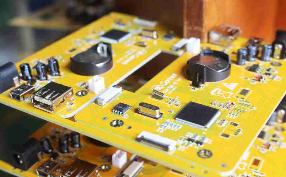
Step 5: Component Assembly
Once the PCB has passed all quality checks, it moves on to the gathering arrange. In this step, the components are fastened onto the PCB. There are two primary strategies of component assembly:
• Surface Mount Technology (SMT): In SMT, little components are set straightforwardly onto the surface of the PCB. This is the most common strategy for high-volume generation due to its speed and precision.
• Through-Hole Technology (THT): In THT, components with leads are embedded into gaps on the PCB and patched from the inverse side. This strategy is ordinarily utilized for bigger components or when a more grounded association is required.
Once the components are set on the board, a reflow fastening prepare is utilized to soften patch glue, which cements to make electrical associations between the components and the PCB.
Step 6: Last Testing and Inspection
After the components are patched, the PCB electronic board goes through extra testing to guarantee that the gathering is redress and the board capacities legitimately. This incorporates utilitarian testing, electrical testing, and visual assessments. If any issues are found, the board is either repaired or rejected.
Step 7: Bundling and Shipping
Once the board passes all tests, it is cleaned, bundled, and arranged for shipping. Defensive coatings are in some cases connected to shield the board from natural components like dampness and clean amid transport.
Conclusion
The PCB electronic board manufacturing prepare is a profoundly point by point and exact operation that requires skill and state-of-the-art gear. From plan and fabric choice to the last get together, each arrange is significant to guaranteeing the quality and usefulness of the PCB. Understanding the manufacturing handle gives us a more prominent appreciation for the complexity and significance of PCBs in the advanced electronic world.
Latest Blog
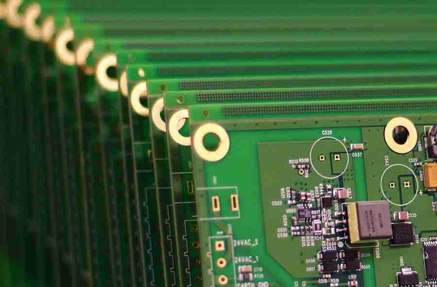
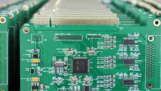
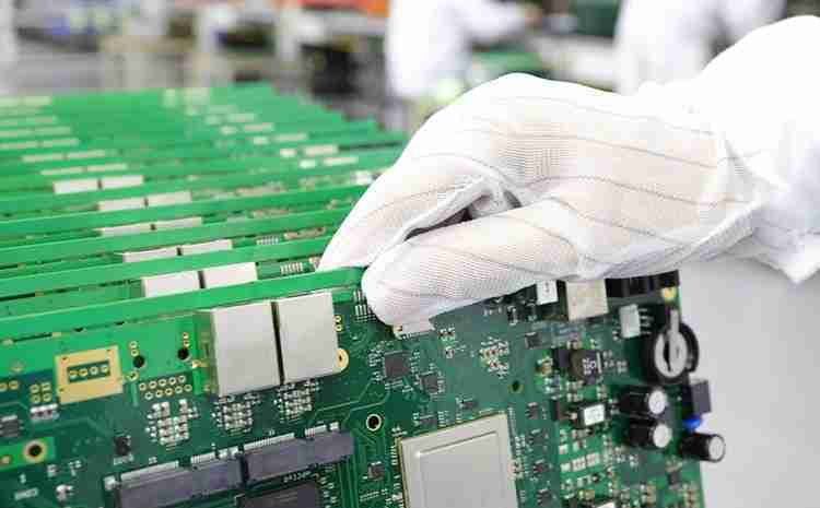

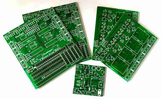
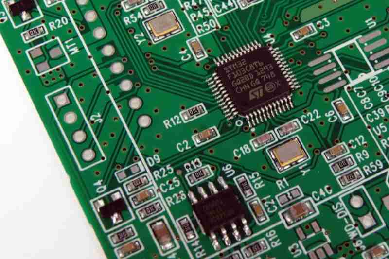
Table of Content
Contcat Us
Phone: +86-18123905375
Email: sales@circuitcardassembly.com
Skype: ali_youte
WhatsApp: +86-18123905375
Wechat: +86-18123905375

 Afrikaans
 Shqip
Shqip አማርኛ
አማርኛ العربية
 Հայերեն
 Azərbaycan dili
 Euskara
 Беларуская мова
 বাংলা
বাংলা Bosanski
 Български
 Català
 Cebuano
 Chichewa
 简体中文
简体中文 繁體中文
繁體中文 Corsu
Corsu Hrvatski
 Čeština
 Dansk
Dansk Nederlands
 Esperanto
 Eesti
Eesti Filipino
 Suomi
Suomi Français
 Frysk
Frysk Galego
 ქართული
 Deutsch
 Ελληνικά
 ગુજરાતી
 Kreyol ayisyen
 Harshen Hausa
 Ōlelo Hawaiʻi
 עִבְרִית
 हिन्दी
 Hmong
Hmong Magyar
 Íslenska
 Igbo
Igbo Bahasa Indonesia
 Gaeilge
 Italiano
 日本語
日本語 Basa Jawa
 ಕನ್ನಡ
ಕನ್ನಡ Қазақ тілі
 ភាសាខ្មែរ
 한국어
한국어 كوردی
كوردی Кыргызча
 ພາສາລາວ
 Latin
Latin Latviešu valoda
 Lietuvių kalba
 Lëtzebuergesch
 Македонски јазик
 Malagasy
 Bahasa Melayu
 മലയാളം
 Maltese
 Te Reo Māori
 मराठी
मराठी Монгол
 ဗမာစာ
ဗမာစာ नेपाली
 Norsk bokmål
 پښتو
پښتو فارسی
فارسی Polski
 Português
 ਪੰਜਾਬੀ
 Română
 Русский
 Samoan
 Gàidhlig
 Српски језик
 Sesotho
 Shona
Shona سنڌي
سنڌي සිංහල
සිංහල Slovenčina
 Slovenščina
 Afsoomaali
 Español
 Basa Sunda
 Kiswahili
 Svenska
 Тоҷикӣ
 தமிழ்
தமிழ் తెలుగు
 ไทย
ไทย Türkçe
 Українська
 اردو
اردو O‘zbekcha
 Tiếng Việt
 Cymraeg
 isiXhosa
 יידיש
יידיש Yorùbá
 Zulu
Zulu