
Electronic gadgets have gotten to be an crucial portion of advanced life, from smart phones and computers to medical hardware and mechanical apparatus. Behind the consistent operation of these gadgets lies a modern and interconnected framework of components, basically driven by Printed Circuit Boards (PCBs) and their assemblies, known as PCBA (Printed Circuit Board Assembly). Understanding how PCB and PCBA work together in electronic circuit plan and Assembly is imperative to increasing in value their part in modern technology.
The Part of PCBs in Electronics
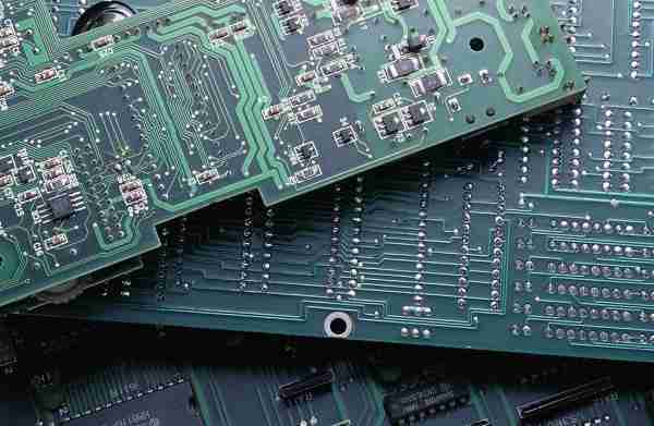
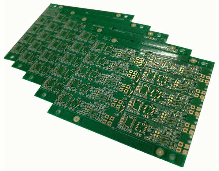
A PCB, or Printed Circuit Board, serves as the spine of present day hardware. It is a level, unbending board made of protection materials with conductive pathways carved onto its surface. These conductive pathways, or follows, give electrical network between diverse components mounted on the board.
• Substrate Fabric: The base of the PCB is as a rule made of a fabric like fiberglass or epoxy gum, guaranteeing solidness and insulation.
• Copper Layers: Lean layers of copper are carved into circuit designs to make conductive paths.
• Solder Veil: A protective layer, known as patch veil, covers the copper follows to anticipate inadvertent brief circuits or oxidation.
• Silkscreen: The silkscreen includes names and images on the board to help Assembly of printed circuit Boards and investigating processes.
The essential work of a PCB is to organize and interface different electronic components into a utilitarian framework, giving a solid and compact structure for electronic circuits.
The Transition from PCB to PCBA
While a PCB is an empty board with circuit pathways, its genuine potential is realized as it were after it is populated with electronic components—this is where the PCBA circuit board comes into play.
What is PCBA? PCBA, or Printed Circuit Board Assembly, alludes to the handle of mounting and fastening components such as resistors, capacitors, diodes, coordinates circuits, and connectors onto the PCB. The last Assembly of printed circuit Boards includes different steps, from putting the components to guaranteeing electrical and utilitarian reliability.
• Component Arrangement: Components are put on the board either physically or utilizing computerized machinery.
• Soldering: Methods such as wave patching, reflow fastening, or manual patching guarantee components are safely attached.
• Inspection: Testing strategies like Automated Optical Inspection (AOI) and X-ray reviews confirm that associations are precise and functional.
• Testing: Electrical testing guarantees that the PCBA capacities as planning, completing the handle of turning a basic PCB into a utilitarian PCBA circuit board.
How PCB and PCBA Complement Each Other
The cooperative energy between PCB and PCBA is crucial to advanced gadgets. Whereas the PCB gives the stage, the PCBA changes it into an operational framework by joining dynamic and detached components.
1. Plan Integration: The plan of a PCB starts with making a schematic that characterizes the electrical associations and the format of the board. This organize is basic for PCBA because:
• The PCB plan decides the situation of components and their connections.
• Advanced plan program simulates electronic circuits to foresee execution some time recently physical assembly.
2. Miniaturization: Present day hardware require compact and lightweight arrangements. The integration of PCB and PCBA encourages this by:
• Combining multilayer PCBs that pack numerous circuit layers in a single board.
• Utilizing Surface Mount Innovation (SMT), which permits littler components to be mounted straightforwardly onto the board.
3. Unwavering quality: Both PCBs and PCBAs are outlined to meet rigid quality and solidness guidelines, guaranteeing solid execution over different applications:
• PCBs are made from heat-resistant and solid materials that persevere extraordinary conditions.
• The Assembly of printed circuit Boards experiences thorough testing to identify and correct imperfections, guaranteeing longevity.
Manufacturing Forms for PCB and Assembly
The manufacturing of PCBs includes exact forms to make a board that meets the indicated plan and useful requirements:
1. Design to Gerber Record Change: The electronic plan is changed over into Gerber records, which manage the situation of layers, follows, and components.
2. Material Planning: The board’s substrate fabric is prepped with copper cladding on one or both sides.
3. Etching and Cover: Layers of copper are carved to shape conductive ways, and numerous layers are covered to make complex multilayer boards.
4. Drilling and Plating: Gaps for through-hole components and vias are penetrated and plated with conductive material.
5. Finishing: A patch veil and silkscreen are connected to total the PCB fabrication.
PCBA Handle Once the PCB is prepared, it continues to the Assembly stage:
1. Component Sourcing: All required components are sourced, guaranteeing compatibility and quality.
2. Component Situation: Utilizing Choose and Put machines or manual strategies, components are set on the board agreeing to the design.
3. Soldering Techniques:
• Wave Fastening: Utilized for through-hole components, where the board passes over a wave of liquid solder.
• Reflow Fastening: Utilized for SMT components, where patch glue is dissolved in an stove to secure components.
4. Inspection and Testing: AOI, useful testing, and in-circuit testing guarantee the last Assembly is fault-free.
Applications of PCB and PCBA Circuit Boards

PCB and PCBA circuit Boards are the building squares for various industries:
1. Consumer Electronics: Smartphone, tablets, and domestic apparatuses depend on compact and effective PCBA circuit boards.
2. Automotive Industry: PCBAs are fundamentally to vehicle control frameworks, infotainment frameworks, and advanced driver-assistance systems (ADAS).
3. Medical Hardware: Exactness disobedient like heart screens, imaging gadgets, and symptomatic devices depend on high-quality PCBAs.
4. Industrial Automation: PCB and Assembly forms are basic in mechanical autonomy, fabricating frameworks, and IoT devices.
5. Telecommunications: Communication gadgets, base stations, and organizing hardware are fueled by PCBAs.
Innovations in PCB and PCBA
The advancement of innovation proceeds to thrust the boundaries of PCB and PCBA capabilities:
1. Flexible PCBs: Adaptable and rigid-flex PCBs permit plans to twist and adjust to interesting shapes, perfect for wearables and compact devices.
2. HDI (High-Density Interconnect) Boards: Progressed Boards with better lines and spaces empower complex plans with diminished frame factors.
3. Automation in Assembly: Robots and AI-driven assessment frameworks upgrade exactness and proficiency in the Assembly of printed circuit boards.
4. Green Manufacturing: Eco-friendly materials and forms are being received to minimize natural impact.
Challenges and Solutions
While PCB and PCBA forms are exceedingly advanced, challenges persist:
• Component Deficiencies: Vacillations in supply can delay PCBA generation. Collaborative determining with providers mitigates this risk.
• Thermal Management: High-power gadgets require progressed warm arrangements such as warm sinks and warm vias to avoid overheating.
• Electromagnetic Interference (EMI): Appropriate establishing and protecting strategies are utilized to guarantee electromagnetic compatibility.
Conclusion
The transaction between PCB and PCBA is the foundation of electronic circuit plan and Assembly. The PCB gives the basic system, whereas the PCBA breathes life into the circuit by coordination dynamic and detached components. Together, they make solid and effective frameworks that control the cutting edge world. From the conceptual plan to last Assembly of printed circuit Boards, progressions in materials, innovation, and forms proceed to thrust the boundaries of what is conceivable, clearing the way for the another era of electronic advancements.


