
Printed Circuit Board (PCB) manufacturing and assembly are indispensably steps in the improvement of for all intents and purposes all electronic gadgets, from smart phones and medical equipment to restorative hardware and mechanical apparatus. As Technology advances, the request for more productive, dependable, and cost-effective PCB manufacturing and Assembly forms has surged. To meet these requests, producers are turning to progressed procedures that thrust the boundaries of plan, execution, and precision.
This Content investigates how to actualize progressed strategies in PCB manufacturing and assembly, centring on the strategies, advances, and best hones that can upgrade the effectiveness, quality, and unwavering quality of PCB production.
1. Understanding the Basics of PCB Manufacturing and Assembly

Before plunging into progressed methods, it’s critical to get it the principal forms included in PCB manufacturing and assembly.
• PCB Manufacturing: The manufacturing handle includes a few stages, counting plan, fabric determination, creation, and testing. Amid creation, the PCB is made by carving conductive follows on a non-conductive substrate, such as fiberglass. After the PCB is created, it goes through forms like boring, plating, patch veil application, and silkscreen printing.
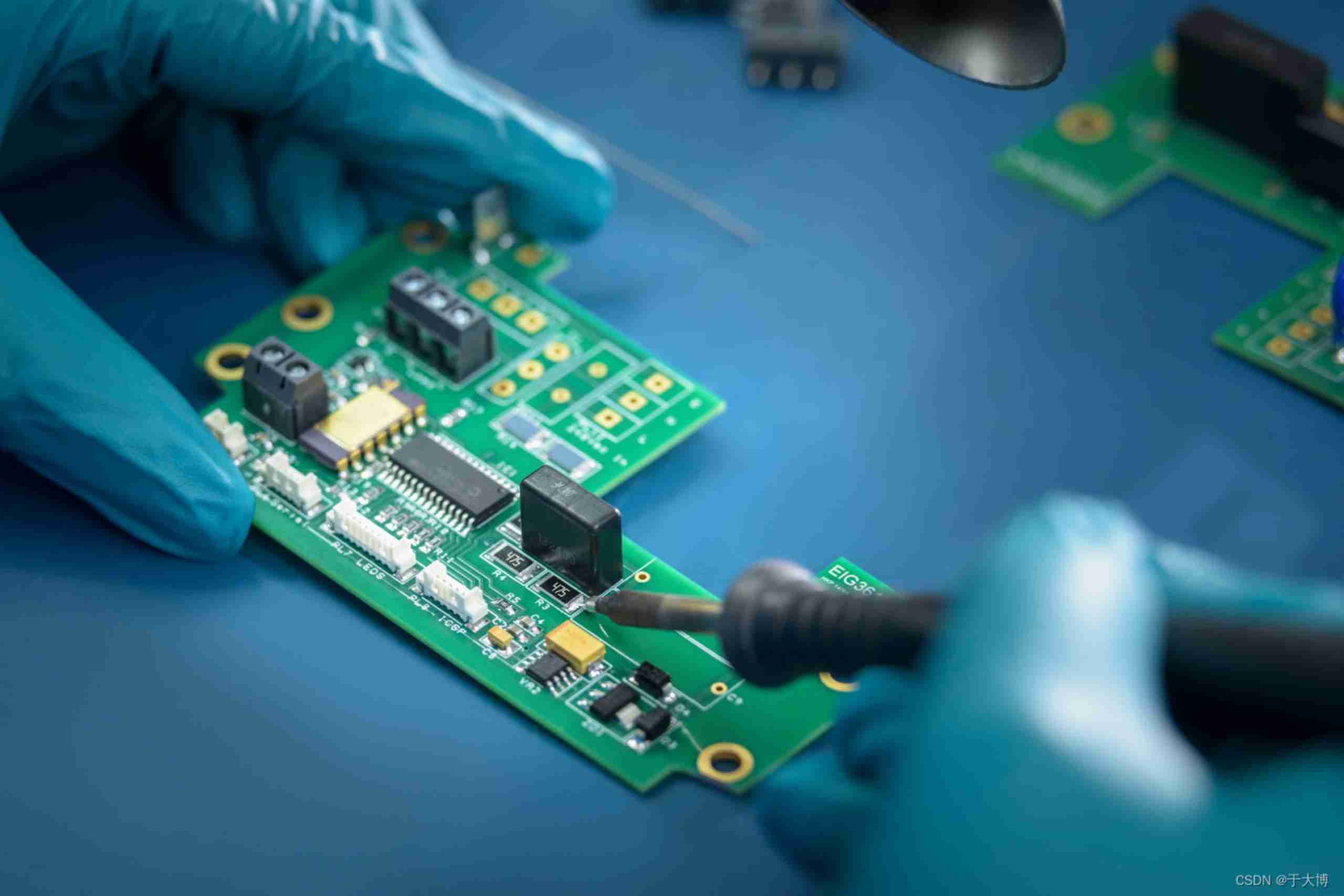
• PCB Assembly: PCB Assembly alludes to the prepare of putting and fastening components onto the created PCB. This can be done through two essential methods:
• Through-Hole Technology (THT): Components with leads are embedded into bored gaps and fastened on both sides of the board.
• Surface Mount Technology (SMT): Components are straightforwardly set on the surface of the PCB, permitting for littler and more thickly pressed designs.
Advanced strategies in both manufacturing and Assembly play a basic part in progressing the execution, lessening costs, and upgrading the adaptability of PCB production.
2. Progressed Methods in PCB Manufacturing
a. High-Density Interconnect (HDI) PCBs
• Implementation: HDI PCBs utilize fine lines, microvias, and stacked vias to make thickly pressed intercontinental. The generation of HDI PCBs ordinarily includes laser boring, which permits for littler gap sizes and more exact vias, empowering a more noteworthy number of components to be put on the board.
• Benefits: HDI PCBs empower quicker information transmission, expanded usefulness, and littler frame components, making them fundamental for cutting edge, high-performance electronic devices.
b. Multilayer PCBs
• Implementation: Manufacturing multilayer PCBs requires cautious arranging of the layer stack-up, arrangement, and by means of plans. The layers are ordinarily reinforced utilizing epoxy or other cements and at that point passed through a cover prepare. Amid this arrange, the PCB experiences warm and weight to guarantee appropriate holding of layers.
c. Progressed Fabric Selection
The choice of fabric plays a pivotal part in the execution and strength of the PCB. The choice of high-performance materials, such as high-frequency covers or ceramic substrates, can altogether progress flag judgment, warm administration, and generally performance.
• Implementation: Progressed materials are frequently chosen based on the particular necessities of the gadget, such as high-speed flag transmission, high-frequency operations, or resistance to extraordinary temperatures.
• Benefits: By utilizing progressed materials, producers can create PCBs that meet the rigid execution prerequisites of high-speed information preparing, broadcast communications, and car applications.
3. Progressed Strategies in PCB Assembly
a. Surface Mount Technology (SMT)
Surface Mount Technology (SMT) is a broadly utilized and progressed assembly strategy for mounting electronic components specifically onto the surface of the PCB. SMT permits for littler components, quicker assembly times, and more proficient utilize of space.
• Implementation: The SMT prepare includes putting components on the PCB utilizing computerized pick-and-place machines, taken after by patching utilizing a reflow fastening handle. The components are regularly set on both sides of the board, permitting for higher component densities.
• Benefits: SMT empowers the generation of compact, high-performance sheets, lessening the by and large measure of the last item. It moreover speeds up the assembly prepare, decreases human mistake, and improves the unwavering quality of the last product.
b. Automated Optical Inspection (AOI)
Automated Optical Assessment (AOI) is an progressed method utilized to assess the quality of PCB assemblies by outwardly checking the components and patch joints on the PCB.
• Implementation: AOI frameworks utilize high-resolution cameras and modern program to distinguish absconds such as fastening issues, component misalignment, or lost components. The framework compares the board’s highlights against predefined details and banners any discrepancies.
• Benefits: AOI moves forward the quality and unwavering quality of the last PCB assembly by identifying surrenders early in the prepare. It moreover decreases the require for manual reviews, which can be time-consuming and error-prone.
c. Particular Soldering
Selective patching is an progressed Assembly strategy utilized for fastening components that cannot be handled utilizing conventional wave fastening strategies, such as through-hole components or touchy components on high-density PCBs.
• Implementation: In specific fastening, a automated arm applies patch to particular regions of the PCB utilizing a accurately controlled handle. This procedure permits for precise fastening of components whereas anticipating harm to adjacent components.
• Benefits: Particular fastening makes strides the exactness and quality of patch joints, especially in ranges with complex or firmly stuffed components. It too permits for more productive and speedier Assembly of complex boards.
d. 3D Printing for PCB Prototyping
3D printing, or added substance manufacturing, is picking up footing in PCB prototyping, empowering creators to make fast models of PCBs and components without the required for conventional manufacturing methods.
• Implementation: 3D printing permits for the creation of custom PCB plans in a division of the time compared to conventional strategies. It can moreover be utilized for creating models of complex 3D structures or cross breed gadgets that coordinated PCBs with mechanical components.
• Benefits: 3D printing quickens the prototyping handle, empowering speedier emphasis and more inventive plan conceivable outcomes. It’s particularly valuable for low-volume generation or when quick turnaround times are required.
4. Best Practices for Implementing Advanced Techniques
To effectively actualize progressed procedures in PCB manufacturing and Assembly, producers must take after best hones to guarantee high-quality, dependable comes about. Here are a few key considerations:
a. Design for Manufacturability (DFM)
Design for Manufacturability (DFM) is a basic angle of actualizing progressed procedures. DFM includes planning PCBs with thought for ease of manufacturing, assembly, and testing. This approach minimizes generation costs, decreases abandons, and moves forward the by and large quality of the last product.
b. Testing and Quality Control
Thorough testing is basic to guarantee the unwavering quality and execution of PCBs. Producers ought to actualize progressed testing strategies such as Functional Testing (FT), In-Circuit Testing (ICT), and X-ray Review to confirm that the PCBs meet the required specifications.
c. Persistent Prepare Improvement
To remain competitive and keep up high-quality measures, producers must receive a culture of nonstop handle change. Routinely investigating and optimizing manufacturing forms, executing modern technologies, and preparing representatives on progressed methods can offer assistance accomplish superior comes about and decrease waste.
Conclusion
Implementing progressed procedures in PCB manufacturing and Assembly is fundamental for assembly the expanding request for high-performance, dependable, and cost-effective electronic gadgets. From High-Density Interconnect (HDI) PCBs and multilayer plans to Surface Mount Technology (SMT) and mechanized review frameworks, these methods play a essential part in improving the proficiency, quality, and versatility of PCB generation.


