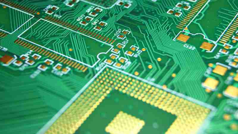
A PCB made from solder paste that does not contain lead during the solder paste printing process is called a lead-free PCB.
In previous PCB manufacturing, solder of PCB contained lead because of its good solderability and low cost. Lead is harmful to our health and development and is not environmentally friendly, although it is not reflected in the electronic products I use daily. Lead in discarded electronic products will pollute the environment. Protecting the environment is our responsibility and a great challenge facing the times.
In response to the Restriction of Hazardous Substances Directive (ROHS) proposed by the EU, our company launched lead-free PCB assembly services to contribute to environmental protection.
Importance of Lead-Free PCB
There are similar ROHS regulations global now, so when manufacturing PCBs or selling electronic products, lead-free should be a key consideration factor. Failure to comply with ROHS regulations may result in significant losses in company profits. Using lead-free solder to assemble PCBs has the following benefits:
• Protect environment
Reducing lead in PCBs helps prevent lead from contaminating land, air, and water, thereby protecting wildlife and human health. Discarded lead-free PCBs should be recycled, which can reduce electronic garbage and ensure an adequate supply of scarce electronic resources.
• Protecting workers health
Contact with lead can cause abnormalities in our body, such as headaches, fatigue, memory loss, and even infertility. The production of lead-free printed circuit boards meets the ROHS standards and protects our health from harm.
• Special Region Sales
The sale of PCB products is prohibited in EU countries that do not meet the ROHS standard. Therefore, producing lead-free printed circuit boards and selling them in these economically developed regions will get high profits.
• Technological progress
Engineers are constantly exploring technologies for producing lead-free PCBs, such as lowering process temperatures, improving mechanical properties, and developing lead-free solders to reduce costs.
Lead-free solder vs Lead solder
| project | Lead-free solder | Lead solder |
| Main Ingredients | Tin, silver, copper | Tin, Lead |
| Melting point | High (217 degrees) | Low (183 degrees) |
| Wettability | Poor (indicates that the weld joint is more solid) | better |
| Strength and hardness | Higher (can withstand l heavy mechanical and thermal stress) | Poor |
| Mechanical behavior | Lead-free solder is higher than lead-containing solder | |
| cost | Higher | Low |
| Applicable performance | Environmentally friendly and recyclable | poisonous |
In summary, Comparing the physical and chemical properties of solder, the process advantages of lead-free PCB are greater than those of lead-containing PCB, especially in terms of environmental protection and soldering quality. So, many electronic equipment manufacturers are choosing lead-free processes to manufacture circuit boards. At the same time, they face many challenges, such as temperature adjustment and equipment upgrades.
If you purchase our lead-free PCB service, you don’t need to worry about the above issues at circuitcardassembly. We have a lot of lead-free PCB manufacturing and assembly cases, a professional team, and advanced welding equipment to ensure you get high-quality products.
Lead-free PCB assembly
• Material analysis and inspection
Before officially starting PCB assembly, component inspection is necessary to ensure that components are made of lead-free materials. Because lead-free components are easily affected by moisture, manufacturers should bake them in an oven.
• Solder Paste Inspection
Check the PCB outline and solder paste according to IPC-610D standards. Humidity levels are also tested in this step because the circuit board is exposed to high humidity in lead-free soldering compared to traditional soldering. After the above steps are completed, PCB assembly can begin.
• Solder Paste Printing
Place the lead-free template on the circuit board and apply the solder paste evenly. The general lead-free solder paste material is SAC305 solder paste.
• SMT Assembly
After applying solder paste, automated machines will mount the electronic components on the circuit board.
• Welding
This stage uses lead-free through holes or hand-welded. No matter which soldering method is used, SMT or THT, soldering must be lead-free.
• Reflow
Place the PCB board in the reflow oven, then under the high-temperature solder paste will melt, and the melted solder paste will cool and solidify at room temperature, which will help fix the electronic components on the circuit board.
• Test packaging
According to IPC-600D standards, test solder joints of lead-free PCB. AOI, X-ray, and visual inspection are used. Before packaging, test the functionality of printed circuit boards.
Our Lead-Free PCB Services
• Lead-free printed circuit boards
• Turnkey Lead-Free PCB Assembly
• Lead-free PCB assembly
• Lead-free SMT assembly
• Lead-free wave soldering
• Lead-free materials
• Lead-free rework
When to Buy Lead-Free PCB Assembly Services
If you have the following concerns, lead-free PCB service will be good for you.
You are selling products in a country or region that has regulatory requirements for lead use, such as the European Union.
• Your local government requires lead-free processes, such as California, USA.
• You are concerned about the potential financial loss from products containing lead.
• You are concerned about the health of your customers who use electronic products that contain Pb
• Lead-free PCB is the development trend, and you don’t want to miss the economic trend.
Summary
Green development is a social trend. As a member of nature, it is our responsibility to protect the environment. Lead-free PCB not only meets regulatory requirements but also has the characteristics of safety and environmental protection. It has a very bright future in the future electronics industry. At the same time, it also faces many challenges.


