
Printed Circuit Boards (PCBs) are the spine of present day gadgets, giving mechanical bolster and interfacing electronic components through conductive pathways. The fabricating, planning, and making of PCB sheets require accuracy, specialized mastery, and progressed apparatus. In this article, we will dig profound into the world of PCB manufacture, plan forms, and the part of PCB makers.
Introduction to PCB Fabrication, Design, and Makers
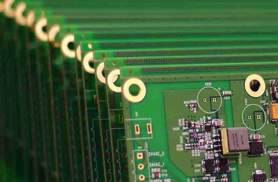
Printed Circuit Boards (PCBs) are fundamental components utilized in for all intents and purposes each electronic gadget, from straightforward contraptions to complex aviation frameworks. The PCB itself is a level board that contains layers of copper conductive tracks and is the establishment upon which distinctive components like resistors, transistors, capacitors, and coordinates circuits are mounted.
The journey of a PCB begins with plan, continues to creation, and concludes with get together and testing. Producers and creators of PCBs must guarantee that these items are not as it were useful but moreover meet the most elevated industry benchmarks for toughness, execution, and safety.
This direct covers the whole PCB prepare, from creation to plan and making, centering on best hones, cutting-edge innovations, and the key players in the industry.
PCB Manufacture: From Concept to Reality
1. Understanding PCB Fabrication
PCB manufacture is the handle of making the real physical circuit board, which serves as the stage for electronic components. The creation prepare includes the taking after key stages:
• Design Approval and Planning: Some time recently generation starts, the plan is carefully inspected for any irregularities or mistakes. This guarantees that the PCB can be manufactured to the correct details given by the designer.
• Substrate Fabric Determination: The base fabric, or substrate, is regularly made of fiberglass, strengthened epoxy tar, or another protection fabric. The most commonly utilized substrate is FR4, which offers a great adjust of electrical execution, taken a toll, and durability.
• Copper Cladding and Designing: PCBs more often than not contain layers of copper thwart on their surface. The copper is covered onto the substrate, and a design is made utilizing a photolithography handle, which exchanges the circuit plan onto the copper.
• Etching: Undesirable copper is expelled utilizing a chemical prepare called carving. As it were the wanted circuit ways, which shape the electrical connections, stay intact.
• Drilling and Plating: Gaps are penetrated to oblige through-hole components or interlayer connections (vias). These gaps are plated with copper to frame conductive connections between the layers of the board.
• Solder Cover Application: A defensive layer known as a patch cover is connected over the copper follows, clearing out the association focuses (cushions) uncovered. The patch cover anticipates brief circuits and gives a visual direct amid component placement.
• Silkscreen Printing: The silkscreen layer contains content and images that give distinguishing proof marks, portion numbers, or names for the components on the PCB.
• Surface Finishing: Different surface finishes like HASL (Hot Air Solder Leveling), ENIG (Electroless Nickel Immersion Gold), or OSP (Organic Solderability Preservative) are applied to protect the exposed copper and enhance solderability.
2. Quality Control and Testing in PCB Fabrication
Once the manufacture handle is total, producers thoroughly test the PCB for quality and execution. Testing strategies include:
• Automated Optical Inspection (AOI): AOI frameworks check the surface of the board to check for any surrenders in the circuit design, such as broken follows or misalignments.
• Electrical Testing: PCBs experience electrical tests to guarantee that there are no open circuits or brief circuits in the design.
• X-ray Inspection: High-end PCBs, especially those with numerous layers, are reviewed with X-rays to confirm the arrangement of inner layers and the astuteness of plated vias.
PCB Circuit Board Plan: Where Innovation Begins
1. Significance of PCB Design
PCB plan is one of the most basic stages in the lifecycle of a printed circuit board. A great PCB plan is fundamental for the usefulness, proficiency, and unwavering quality of the electronic gadget it underpins. Destitute plan can lead to signal impedances, overheating, or indeed disappointment of the device.
Designers utilize specialized computer program to make the format of the circuit, situating all the fundamental components and planning the copper follows that will interface them. This handle requires a profound understanding of both the electrical behavior and physical limitations of the system.
2. Key Steps in PCB Design
a. Schematic Capture
The to begin with step in PCB plan is making a schematic, a graph that speaks to the electrical connections between components. Creators utilize CAD (Computer-Aided Plan) instruments to construct the schematic, characterizing how components like capacitors, resistors, and chip are interconnected.
b. Component Placement
Once the schematic is total, components must be situated on the board. This is a fragile prepare that requires originators to adjust electrical execution with physical limitations. Components like signal keenness, warm administration, and mechanical stretch must be considered.
• Signal Astuteness: High-speed circuits, such as those utilized in broadcast communications, require uncommon consideration to follow lengths and situation to anticipate impedances and signal degradation.
• Thermal Administration: Legitimate component arrangement can offer assistance scatter warm, avoiding components from overheating.
• Mechanical Push: Components ought to be set to minimize mechanical push amid operation, which might lead to wear and possible failure.
c. Routing
Routing is the prepare of drawing the copper follows that will interface the components. Architects must carefully arrange the ways of these follows to dodge crossing over one another. Multi-layer PCBs, which contain numerous stacked layers of copper, permit for more complex routing.
d. Design Rule Check (DRC)
After steering, the plan experiences a Design Rule Check (DRC) to guarantee that it meets particular industry benchmarks and producer limitations. These rules cover viewpoints like least follow width, dividing between follows, and the estimate of penetrated gaps.
e. Signal Reenactment and Analysis
Signal recreation devices offer assistance creators foresee how the circuit will carry on in the genuine world. They can recreate variables like signal reflection, crosstalk, and control conveyance, making a difference creators make any essential changes some time recently fabrication.
3. PCB Plan Computer program Tools
Designing a PCB requires effective and natural program apparatuses. A few of the most well known PCB plan program bundles include:
• Altium Architect: A profoundly progressed apparatus that gives schematic capture, PCB format, and recreation in one bundle. It is broadly utilized in proficient situations due to its capable features.
• Eagle: Known for its user-friendly interface, Hawk is prevalent among both specialists and experts. It incorporates a huge library of components and is profoundly customizable.
• KiCAD: An open-source choice that gives comparative usefulness to Altium and Hawk but is accessible for free. It’s a prevalent choice for new businesses and little businesses.
• OrCAD: Another professional-grade instrument, OrCAD is known for its vigorous reenactment capabilities and broad library of components.
PCB Board Makers: Turning Designs Into Reality
1. The Part of PCB Makers
PCB producers, or producers, are mindful for turning a plan into a physical item. They take the plan records given by the PCB architect, plan the essential materials, and utilize progressed fabricating hardware to create the PCB.
Manufacturers offer an extend of administrations, from model generation to high-volume fabricating. Numerous producers moreover give gathering administrations, where they put and patch components onto the PCB, making a total electronic device.
2. Key Contemplations for Choosing a PCB Manufacturer
Selecting the right PCB producer is basic for the victory of any hardware extend. Here are a few key components to consider:
• Capabilities: Distinctive producers specialize in diverse sorts of PCBs, such as single-layer, multi-layer, or adaptable sheets. It’s imperative to select a producer that can handle the particular needs of your design.
• Turnaround Time: For time-sensitive ventures, choosing a producer with quick turnaround times is basic. A few producers offer assisted administrations for an extra fee.
• Quality Assurance: Guarantee that the producer has a solid quality confirmation prepare in put, counting review and testing at each organize of production.
• Cost: Whereas cost is continuously a thought, it’s imperative to keep in mind that the cheapest alternative isn’t continuously the best. High-quality PCBs may fetched more forthright but can spare you cash in the long run by diminishing the chance of absconds or failures.
• Certifications: See for producers with certifications such as ISO 9001 or IPC (Organized for Printed Circuits) benchmarks, which illustrate their commitment to quality.
3. Prototype vs Production PCBs
Many PCB producers offer two primary administrations: model and generation PCBs. Prototyping is the prepare of making a little clump of PCBs for testing and approval. Generation, on the other hand, includes fabricating bigger amounts for commercial use.
a. Prototype PCBs
Prototype PCBs are fundamental for confirming the plan and guaranteeing it works as anticipated. These PCBs are regularly made in little amounts, which permits originators to recognize and adjust any issues some time recently moving to full-scale production.
Prototype administrations regularly have speedier turnaround times and are more adaptable in terms of plan changes.
b. Production PCBs
Once the model has been approved, the another step is generation. This includes fabricating PCBs in expansive amounts, regularly in the thousands or millions, depending on the application. Generation PCBs must meet strict quality guidelines to guarantee steady execution over each board.
What is a Printed Circuit Board (PCB)?
A Printed Circuit Board (PCB) is a board that mechanically underpins and electrically interfaces electronic components utilizing conductive pathways, tracks, or signal follows carved from copper sheets covered onto a non-conductive substrate. PCBs are principal to the operation of electronic gadgets, as they give the framework for signals to stream and components to communicate effectively.
Types of PCBs
PCB producers deliver different sorts of sheets depending on the necessities of the gadget they will be utilized in. Here are a few common types:
1. Single-Layer PCB: Contains as it were one layer of conductive fabric, making it reasonable for straightforward devices.
2. Double-Layer PCB: Highlights two layers of conductive fabric, permitting for more complex designs.
3. Multilayer PCB: Incorporates three or more conductive layers, utilized in progressed gadgets that require tall usefulness in little spaces.
4. Rigid PCBs: Made from strong substrate fabric and outlined to be inflexible.
5. Flexible PCBs: Made from adaptable materials that permit twisting without breaking.
6. Rigid-Flex PCBs: Combines both inflexible and adaptable circuits, permitting for energetic bowing and adaptability inside the design.
The PCB Fabricating Process
The prepare of PCB fabricating includes a few stages, from plan to testing. Here’s a streamlined adaptation of the commonplace steps a PCB producer follows:
1. Design and Format: The plan of the PCB is made utilizing specialized computer program like Hawk or Altium. This plan incorporates the course of action of components and the situation of conductive traces.
2. Printing the Design: Once the format is total, the plan is printed onto the copper layer. Depending on the complexity, this can include different layers being printed in alignment.
3. Etching: Undesirable copper is evacuated from the board, clearing out as it were the wanted copper follows that shape the electrical connections.
4. Drilling: Gaps are bored into the PCB where components such as resistors and capacitors will be embedded. For multilayer PCBs, this step is pivotal to guarantee network between layers.
5. Plating and Solder Mask Application: The penetrated gaps are plated, and a patch cover is connected to secure the copper follows and avoid brief circuits amid soldering.
6. Component Arrangement and Patching: Electronic components are set onto the board, and fastening is utilized to interface them to the copper traces.
7. Testing and Quality Control: At long last, the PCB experiences thorough testing to guarantee it capacities as planning. This may incorporate visual reviews, electrical tests, and useful tests.
The Importance of Choosing the Right PCB Manufacturer
Selecting the right PCB manufacturer is a crucial decision that can significantly impact the success of a product. Here are some factors to consider when choosing a Printed Circuit Manufacturer:
1. Quality Control: Ensuring the manufacturer follows strict quality control measures is essential. Look for manufacturers with ISO certification and a proven track record of delivering high-quality products.
2. Capabilities: Different manufacturers specialize in different types of PCBs. Choose a manufacturer that has experience in producing the type of board you need, whether it’s a simple single-layer board or a complex multilayer or flexible PCB.
3. Lead Time: Time-to-market is critical in many industries. Choose a manufacturer that can meet your production timelines, whether you need quick-turn prototypes or large-scale production.
4. Cost: While cost shouldn’t be the only consideration, it’s important to find a manufacturer that offers competitive pricing without compromising on quality.
5. Customer Support: A good PCB manufacturer should provide excellent customer support, including technical assistance during the design phase, transparent communication throughout the manufacturing process, and after-sales service.
Conclusion
The world of Printed Circuit Board manufacturers is diverse and dynamic, with many companies offering a wide range of services to meet the needs of different industries. Whether you’re developing a simple consumer electronic device or a sophisticated aerospace system, choosing the right PCB manufacturer can make all the difference in terms of quality, performance, and reliability.
The top manufacturers in the industry are continually innovating, adopting new technologies, and improving their processes to stay competitive. As the demand for advanced electronics grows, so does the need for high-quality, reliable PCBs. By partnering with the right manufacturer, you can ensure your products meet the highest standards and stand out in today’s competitive market.


