
Top PCB Board Maker & Fabrication: Leading Manufacturer for Quality PCB Solutions
Printed Circuit Boards (PCBs) have revolutionized the gadgets industry, shaping the spine of most advanced gadgets. From basic shopper contraptions to complex mechanical machines, PCBs give the vital back and network for electronic components. This article plunges profound into PCB circuit board design, the role of PCB makers, the intricacies of PCB fabrication, and the crucial role that PCB fabrication manufacturers play in the electronics ecosystem.
1. Understanding PCB Circuit Board Design
What is PCB Design?
PCB design alludes to the handle of laying out a physical circuit board that underpins and interfaces electronic components. The plan ordinarily includes making a schematic, selecting materials, characterizing follows courses, and planning the board for creation. PCBs can extend from basic single-layer plans to more complex multi-layer boards.
The PCB design handle is basic since it guarantees that the last item will work as expecting. A well-designed PCB will bolster flag judgment, effective control dispersion, and mechanical strength.
Steps Included in PCB Design
1. Conceptualization and Schematic Design:
The to begin with step in PCB plan includes making a schematic. A schematic is basically the outline of your circuit. Engineers will layout which components are required and how they ought to be associated. This step is ordinarily done utilizing PCB plan computer program like Altium Architect, Falcon, or KiCad.
2. Component Placement:
Once the schematic is total, the another step is setting components on the board. Component arrangement is basic since it influences the board’s usefulness, execution, and ease of make. Components like resistors, capacitors, and integrated circuits (ICs) require to be set in a way that minimizes follow lengths and diminishes electromagnetic interference.
3. Routing of Traces:
After component situation, the following step is steering the follows. These follows are the physical copper pathways that interface diverse components. Architects require to guarantee that the follows are wide sufficient to carry the required current but little sufficient to fit inside the accessible space.
4. Design Rule Check (DRC):
A Design Rule Check is a computerized prepare that guarantees the plan meets particular electrical and fabricating limitations. It checks for issues like follow width infringement, brief circuits, and dividing problems.
5. Generating the Bill of Materials (BOM):
The BOM is a comprehensive list of all the components that will be utilized in the PCB. It incorporates portion numbers, amounts, and depictions, which are basic for obtainment and assembly.
6. Gerber Record Generation:
The last arrange in PCB plan is creating the Gerber records. Gerber records are the standard record arrange utilized by PCB manufacture producers. They incorporate data almost the copper layers, patch veil, silkscreen, and bore holes.
Best Practices in PCB Design
• Minimize Crosstalk: Keep high-speed signals absent from delicate analog circuits to decrease crosstalk and flag interference.
• Proper Establishing: Utilize a strong ground plane to guarantee great flag astuteness and decrease noise.
• Thermal Administration: Guarantee that components with tall warm scattering, such as control controllers and chip, have satisfactory warm sinks or warm vias.
• Design for Manufacturability (DFM): Continuously plan the PCB with fabricating imperatives in intellect, guaranteeing that the board can be effectively fabricated.
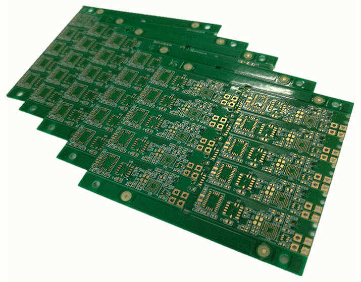
2. Role of PCB Board Maker
Who is a PCB Board Maker?
A PCB board maker is a company or person that specializes in planning and creating printed circuit sheets. These producers are frequently a basic interface in the supply chain, making a difference to decipher a designer’s thoughts into physical sheets that can be utilized in electronic devices.
Services Advertised by PCB Board Makers
1. Prototyping:
Many PCB makers offer prototyping administrations that permit engineers to test their plans some time recently mass generation. PCB Prototyping is a fundamental portion of the improvement handle, as it makes a difference capture potential issues early on.
2. Customization:
PCB producers can customize sheets based on the client’s necessities. This can include altering the board’s measurements, layer number, fabric sort, or follow thickness.
3. Component Sourcing:

In expansion to making the PCB, numerous makers offer component sourcing administrations. This can spare engineers and businesses critical time and exertion by bundling component obtainment with PCB manufacturing.
4. Assembly:
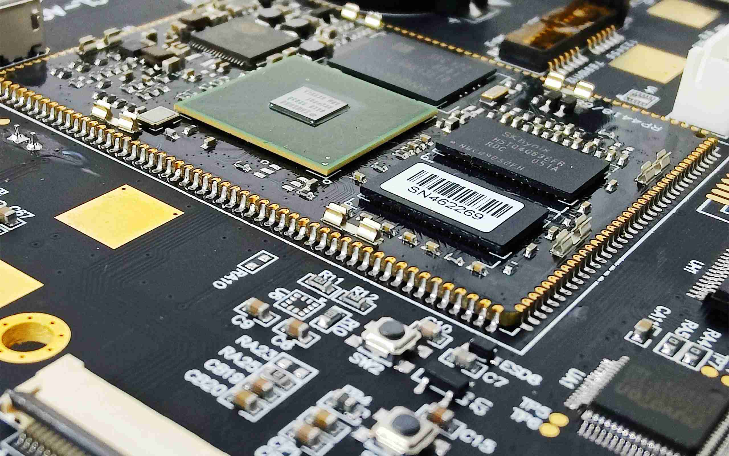
Some PCB makers to give PCB assembly administrations, where they put components on the board and patch them in put. This is known as PCBA (Printed Circuit Board Assembly).
Choosing the Right PCB Maker
Selecting the right PCB producer is significant for the victory of yours extend. A few key variables to consider include:
• Experience: Select a producer with broad involvement in your particular industry or application.
• Quality Affirmation: Guarantee that the maker has thorough quality control forms in put to anticipate fabricating defects.
• Lead Time: Consider how rapidly the producer can provide your sheets, particularly if you’re working on tight venture timelines.
• Cost: Whereas fetched is continuously a figure, make beyond any doubt it doesn’t come at the cost of quality. Cheap PCBs can frequently lead to disappointments in the field.
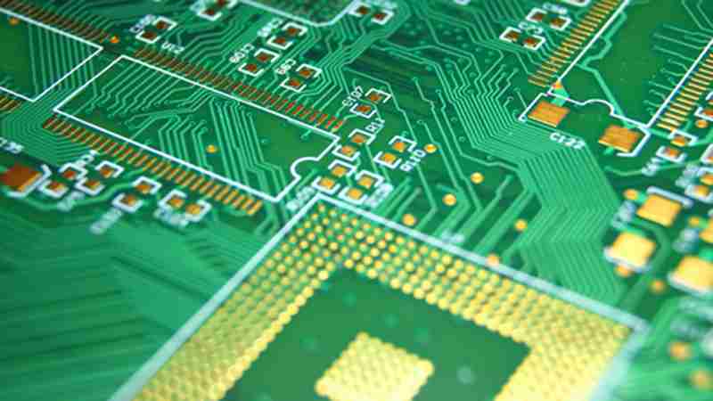
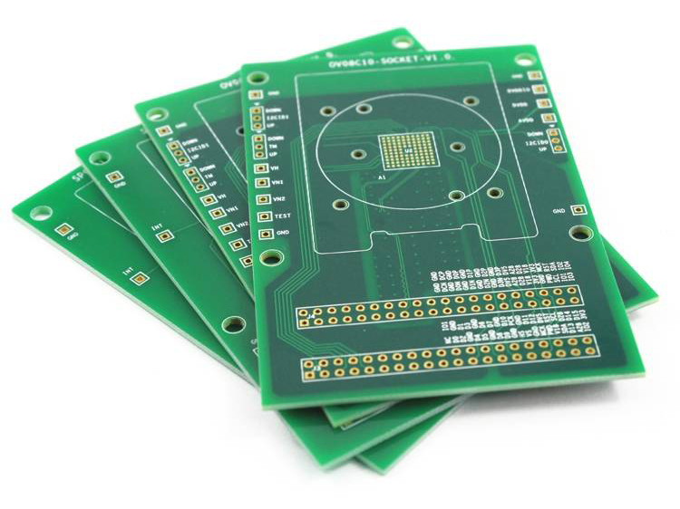
3. PCB Board Fabrication: A Detailed Look
What is PCB Fabrication?
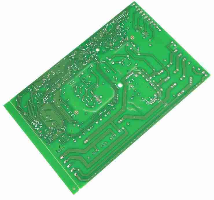
PCB manufacture is the handle of making the genuine printed circuit board from a plan. This prepare includes changing over the plan records (such as Gerber records) into a physical board. PCB creation incorporates different steps, counting carving, layering, penetrating, and applying patch masks.
Materials Utilized in PCB Fabrication
The materials utilized in PCB manufacture can enormously impact the board’s execution. A few common materials include:
• FR4 (Fire Retardant 4): The most common fabric utilized for the PCB substrate, FR4 is a composite fabric made of woven glass and epoxy resin.
• Copper Cladding: PCBs utilize copper to make conductive ways for electrical signals. The thickness of the copper layer can change based on the application.
• Solder Cover: A green (or other colored) polymer layer that ensures the copper follows and avoids brief circuits.
• Silkscreen: The silkscreen layer contains printed data, such as component names and logos, on the board.
Steps in PCB Fabrication
1. Photoplotting and Film Generation:
The to begin with step is to change over the Gerber records into movies. These movies act as veils that will be utilized to exchange the plan onto the PCB substrate.
2. Etching:

During carving, a chemical handle evacuates undesirable copper from the board, clearing out as it were the required follows. This handle makes the circuit ways that will interface the components.
3. Layer Stacking (for Multilayer Boards):
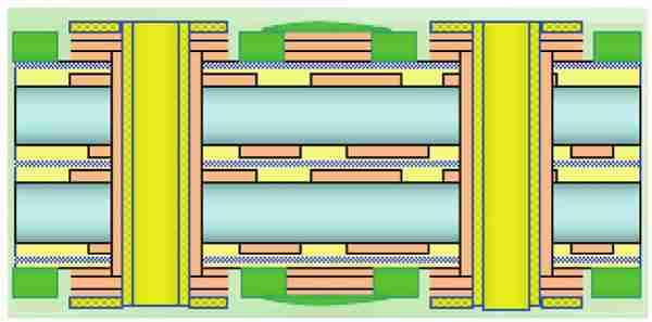
In multilayer PCBs, different layers of carved copper are stacked together. Between each layer, a protection fabric is connected, and the layers are fortified utilizing warm and pressure.
4. Drilling:

Holes are bored into the board for component leads and vias (which interface follows between layers). Exactness is basic in this step; as indeed a little misalignment can render the board unusable.
5. Solder Cover Application:
After boring, the board is cleaned, and a patch cover is connected. The patch veil ensures the copper follows and avoids patch from bridging unintended associations amid assembly.
6. Silkscreen Printing:
The silkscreen layer is included after the patch veil. This layer incorporates reference designators, component diagrams, and other valuable data for assembly.
7. Finishing and Cutting:
The board is wrapped up by applying a surface wrap up (e.g., HASL, ENIG) to ensure the uncovered copper cushions. The last step is cutting the board to its craved dimensions.
Quality Control in PCB Fabrication
Quality control is basic in PCB manufacture. This can incorporate visual reviews, electrical tests (such as flying test or bed-of-nails testing), and indeed X-ray assessment for multilayer sheets. The objective is to guarantee that the board meets the plan determinations and capacities as intended.
4. PCB Manufacture Producer: Key Considerations
What is a PCB Manufacture Manufacturer?
A PCB creation producer is a company that specializes in creating printed circuit sheets at scale. These producers regularly serve a wide run of businesses, from customer gadgets to aviation. They are dependable for turning plan records into physical items that meet exact specifications.
Types of PCB Creation Manufacturers
1. Prototyping Manufacturers:
These producers specialize in small-batch generation and quick-turn prototyping. They are perfect for companies in the R&D stage of item development.
2. High-Volume Manufacturers:
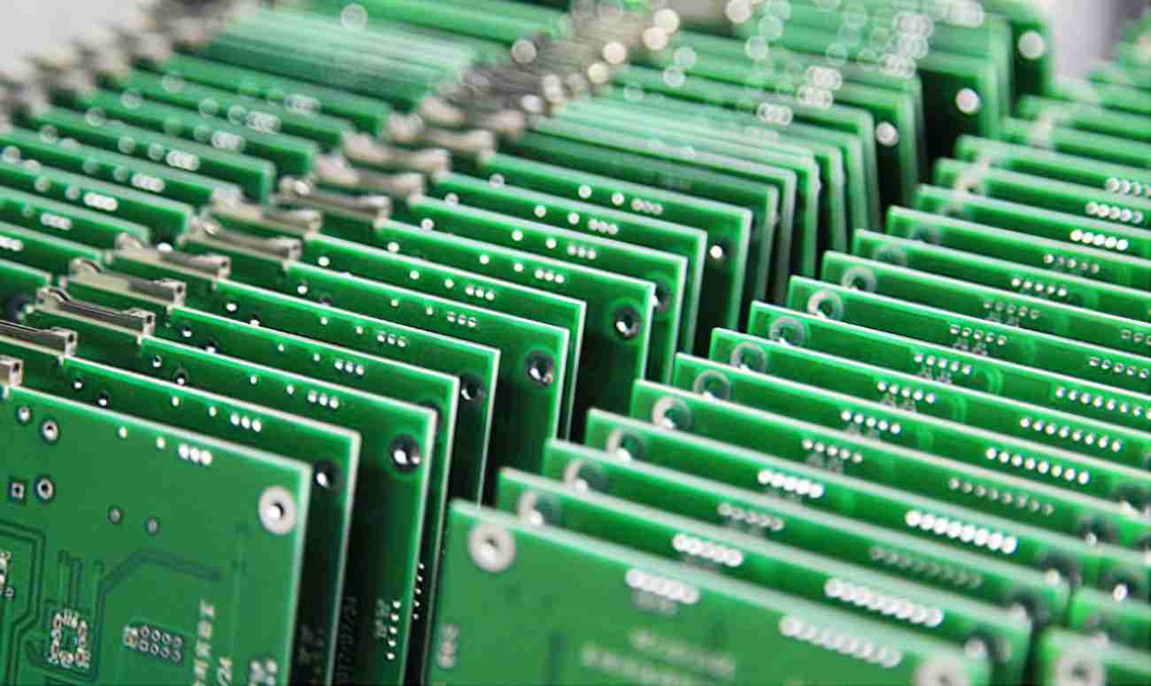
These producers centre on large-scale generation runs. They have the capacity to deliver thousands or indeed millions of PCBs with reliable quality.
3. Specialty Manufacturers:
Some producers specialize in specialty regions, such as adaptable PCBs, rigid-flex PCBs, or high-frequency sheets. These producers utilize specialized forms and materials to meet interesting application requirements.
Factors to Consider When Choosing a PCB Manufacture Manufacturer
1. Technology Capabilities:
The producer must be able to deliver the sort of PCB you require, whether it’s a standard inflexible board or a more complex flex or multilayer board. Make beyond any doubt they have the innovation to handle high-frequency plans, HDI (High-Density Interconnect) necessities, or other extraordinary features.
2. Certifications and Compliance:
Many businesses have strict administrative prerequisites. For illustration, aviation and restorative businesses require PCBs that meet particular certifications like ISO 9001, IPC-6012, or RoHS compliance. Select a producer with the fundamental certifications for your industry.
3. Cost vs. Quality:
While fetched is an imperative thought, it ought to never come at the cost of quality. Second rate PCBs can lead to gadget disappointments, which can be distant more expensive in the long run.
4. Lead Time:
In fast-moving businesses like shopper hardware, time-to-market is vital. Select a producer that can meet your conveyance timelines without compromising on quality.
5. After-Sales Support:
Look for producers that offer after-sales back, such as investigating, disappointment examination, or help with component sourcing.
6. Geographic Location:
While numerous companies select abroad producers for taken a toll reserve funds, there are points of interest to working with nearby producers, such as shorter shipping times and simpler communication.
The Future of PCB Fabrication
As innovation advances, PCB manufacture is too progressing. The rise of progressed fabricating strategies, such as added substance fabricating (3D printing for PCBs), guarantees to alter how circuit sheets are made. Also, there is developing intrigued in eco-friendly PCB fabricating hones, such as utilizing biodegradable materials and lessening squander in the generation process.
Conclusion
The world of PCB plan, creation, and fabricating is both tremendous and complex. From the beginning stages of planning a schematic to the last generation of a circuit board, each step plays a pivotal part in the victory of an electronic gadget. PCB board makers and manufacture producers are key accomplices in this handle, guaranteeing that plans are interpreted into utilitarian, high-quality items. By understanding the subtleties of PCB plan, creation, and fabricating, engineers and businesses can make educated choices that lead to way better execution, lower costs, and quicker time-to-market.
Whether you’re a little start up creating an unused contraption or an expansive organization in require of high-volume PCB generation, choosing the right accomplices in this handle can make all the distinction in the victory of yours extend.
Latest Blog
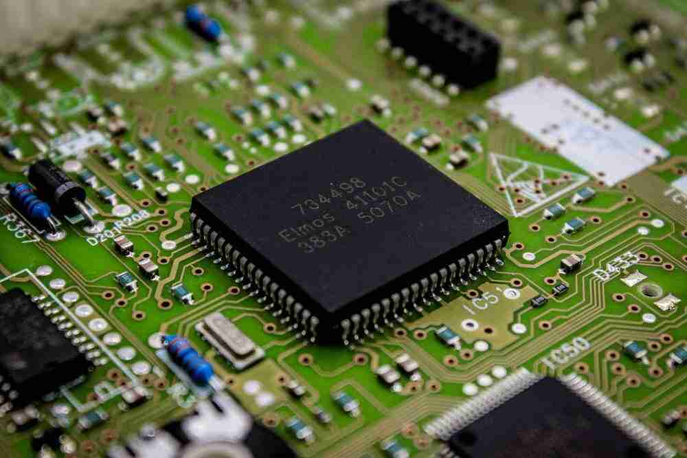
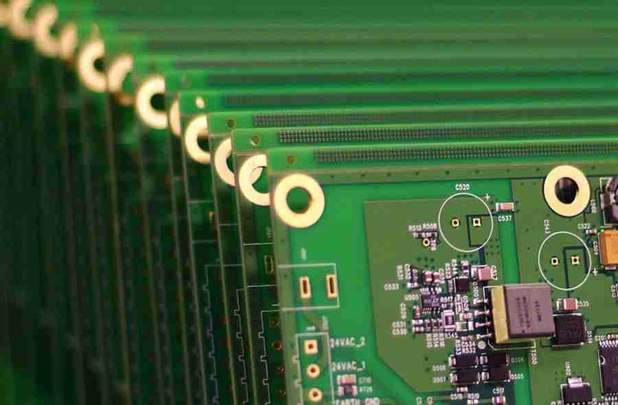
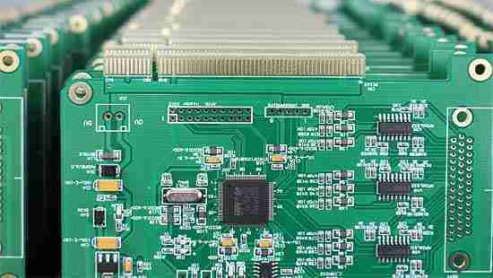
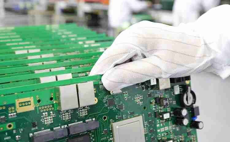

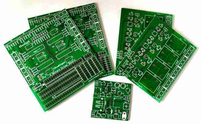
Table of Content
Contcat Us
Phone: +86-18123905375
Email: sales@circuitcardassembly.com
Skype: ali_youte
WhatsApp: +86-18123905375
Wechat: +86-18123905375

 Afrikaans
 Shqip
Shqip አማርኛ
አማርኛ العربية
 Հայերեն
 Azərbaycan dili
 Euskara
 Беларуская мова
 বাংলা
বাংলা Bosanski
 Български
 Català
 Cebuano
 Chichewa
 简体中文
简体中文 繁體中文
繁體中文 Corsu
Corsu Hrvatski
 Čeština
 Dansk
Dansk Nederlands
 Esperanto
 Eesti
Eesti Filipino
 Suomi
Suomi Français
 Frysk
Frysk Galego
 ქართული
 Deutsch
 Ελληνικά
 ગુજરાતી
 Kreyol ayisyen
 Harshen Hausa
 Ōlelo Hawaiʻi
 עִבְרִית
 हिन्दी
 Hmong
Hmong Magyar
 Íslenska
 Igbo
Igbo Bahasa Indonesia
 Gaeilge
 Italiano
 日本語
日本語 Basa Jawa
 ಕನ್ನಡ
ಕನ್ನಡ Қазақ тілі
 ភាសាខ្មែរ
 한국어
한국어 كوردی
كوردی Кыргызча
 ພາສາລາວ
 Latin
Latin Latviešu valoda
 Lietuvių kalba
 Lëtzebuergesch
 Македонски јазик
 Malagasy
 Bahasa Melayu
 മലയാളം
 Maltese
 Te Reo Māori
 मराठी
मराठी Монгол
 ဗမာစာ
ဗမာစာ नेपाली
 Norsk bokmål
 پښتو
پښتو فارسی
فارسی Polski
 Português
 ਪੰਜਾਬੀ
 Română
 Русский
 Samoan
 Gàidhlig
 Српски језик
 Sesotho
 Shona
Shona سنڌي
سنڌي සිංහල
සිංහල Slovenčina
 Slovenščina
 Afsoomaali
 Español
 Basa Sunda
 Kiswahili
 Svenska
 Тоҷикӣ
 தமிழ்
தமிழ் తెలుగు
 ไทย
ไทย Türkçe
 Українська
 اردو
اردو O‘zbekcha
 Tiếng Việt
 Cymraeg
 isiXhosa
 יידיש
יידיש Yorùbá
 Zulu
Zulu