
What Are the Key Stages of PCB Prototype Development?
A PCB (Printed Circuit Board) prototype is an basic step in the electronics improvement prepare, serving as a preparatory form of the last circuit board plan. This significant stage permits engineers to approve their plan concepts, test usefulness, and recognize potential issues some time recently committing to full-scale production.
PCB prototyping regularly starts after schematic plan and format completion. Advanced prototyping strategies incorporate conventional chemical carving, CNC processing, and progressed added substance fabricating strategies. Each approach offers diverse preferences in terms of accuracy, turnaround time, and cost.
When creating a PCB prototype, engineers must consider a few components: component arrangement optimization, flag judgment, warm administration, and manufacturability. The prototype stage frequently includes different cycles as plans are refined based on testing results.
Rapid prototyping administrations have changed the gadgets industry by significantly lessening improvement cycles. What once took weeks can presently be completed in days or indeed hours with progressed administrations advertising same-day turnarounds for basic designs.
Cost contemplations for PCB prototypes incorporate not as it were fabricating costs but moreover the esteem of identifying plan imperfections early. A well-executed prototype stage can avoid expensive mistakes in mass generation, making it a monetarily judicious speculation in spite of the starting expense.
This Substance investigates the key stages of PCB prototype improvement, giving a point by point breakdown of each step included in bringing a circuit board to life.
Stage 1: Conceptualization and Design Requirements
The to begin with arrange in PCB prototype improvement is characterizing the concept and plan prerequisites. This step involves:
● Understanding the application of the PCB.
● Determining electrical and mechanical constraints.
● Defining key details, such as control utilization, flag judgment, and warm management.
● Identifying required components and materials.
Design engineers work closely with clients or venture groups to guarantee that the PCB meets useful and execution requirements.
Stage 2: Schematic Design
The schematic plan is the establishment of the PCB improvement handle. In this stage:
● Engineers utilize Electronic Design Automation (EDA) computer program such as Altium Originator, KiCad, or Hawk to make a circuit diagram.
● Each component is doled out a particular electrical work, and associations between components are defined.
● Engineers conduct starting simulations to confirm circuit performance.
● The schematic is looked into and refined to maintain a strategic distance from plan errors.
A well-drafted schematic guarantees a consistent move to the another arrange of PCB format design.
Stage 3: PCB Layout and Routing
Once the schematic is total, the another step is planning the PCB format. This involves:
● Converting the schematic into a physical board format utilizing PCB plan software.
● Defining layer stack-ups, through arrangements, and follow widths.
● Ensuring legitimate component arrangement to optimize execution and manufacturability.
● Routing electrical follows to minimize impedances and optimize flag integrity.
● Performing Plan Run the show Checks (DRC) to guarantee compliance with fabricating constraints.
Proper format and directing are basic for guaranteeing the PCB’s electrical execution and reliability.
Stage 4: Design Validation and Simulation
Before moving to manufacture, the PCB plan must be approved through reenactments and plan confirmation procedures. This organize includes:
● Signal Keenness Examination: Guarantees negligible flag twisting and crosstalk.
● Power Judgment Investigation: Assesses control conveyance and voltage drop.
● Thermal Examination: Surveys warm scattering to avoid overheating.
● Design Run the Show Confirmation: Guarantees compliance with industry standards.
Simulation makes a difference recognize potential plan issues early, decreasing the hazard of expensive rework.
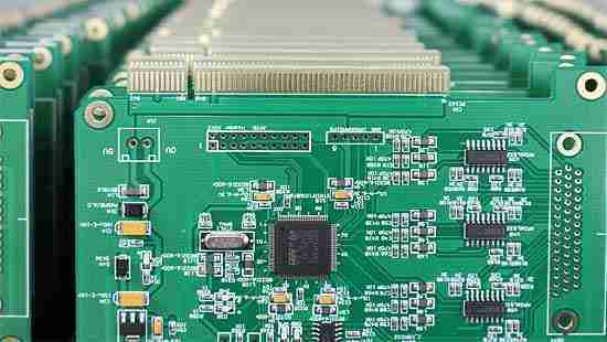
Stage 5: Prototype Fabrication
Once the plan is finalized, the prototype PCB is manufactured. The handle includes:
● Generating Gerber Records: These records contain plan information essential for PCB manufacturing.
● Material Determination: Choosing suitable substrate materials such as FR4, Rogers, or adaptable PCBs.
● PCB Fabricating: Includes carving copper follows, boring gaps, and including surface finishes.
● Solder Veil and Silkscreen Application: Gives security and labeling for components.
● Bare Board Testing: Confirms the astuteness of associations some time recently assembly.
Prototyping producers utilize fast PCB generation methods to make testable circuit sheets quickly.
Stage 6: PCB Assembly
After manufacture, the prototype PCB experiences gathering, which involves:
● Component Sourcing: Guaranteeing high-quality and congruous electronic components.
● Surface Mount Technology (SMT) Gathering: Computerizing component situation for efficiency.
● Through-Hole Technology (THT) Get together: Hand or wave fastening for certain components.
● Reflow Fastening: Dissolving patch glue to frame electrical connections.
● Automated Optical Assessment (AOI): Identifying gathering abandons such as misaligned components.
Proper get together guarantees the prototype capacities as aiming and is prepared for testing.
Stage 7: Functional Testing and Debugging
Once gathered, the PCB prototype is tried to guarantee it meets plan determinations. Testing strategies include:
● Electrical Testing: Checking for coherence, shorts, and appropriate voltage levels.
● Functional Testing: Confirming circuit operation beneath anticipated conditions.
● Environmental Testing: Evaluating execution beneath temperature and mugginess variations.
● Debugging and Fixes: Recognizing and settling issues found amid testing.
This arrange makes a difference refine the plan some time recently moving to full-scale production.
Stage 8: Design Refinement and Iteration
Based on testing criticism, the plan may require alterations. The refinement prepare includes:
● Correcting Plan Imperfections: Tending to distinguished issues in the format or component selection.
● Optimizing Execution: Improving circuit effectiveness and decreasing noise.
● Reducing Fabricating Costs: Disentangling the plan for cost-effective production.
● Creating Extra Prototypes: Approving plan changes some time recently finalization.
Iteration is a pivotal step to guarantee a solid and manufacturable PCB.
Stage 9: Final Prototype Approval
Once all refinements are total, the last prototype undergoes:
● Final Useful Approval: Guaranteeing all execution criteria are met.
● Regulatory Compliance Testing: Assembly industry guidelines such as CE, FCC, or RoHS.
● Customer or Partner Endorsement: Accepting affirmation some time recently mass production.
Approval marks the move from prototyping to generation readiness.
Conclusion
PCB prototype improvement is a multi-stage prepare that requires cautious arranging, plan, approval, and testing. By taking after these key stages—conceptualization, schematic plan, PCB format, approval, creation, gathering, testing, cycle, and approval—engineers can guarantee a high-quality and solid PCB some time recently moving to mass generation. Each step plays a crucial part in minimizing plan blemishes, optimizing execution, and streamlining the fabricating process.
Understanding these stages can offer assistance architects, engineers, and producers create effective and imaginative electronic items that meet industry measures and client desires.
Latest Blog
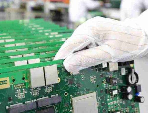
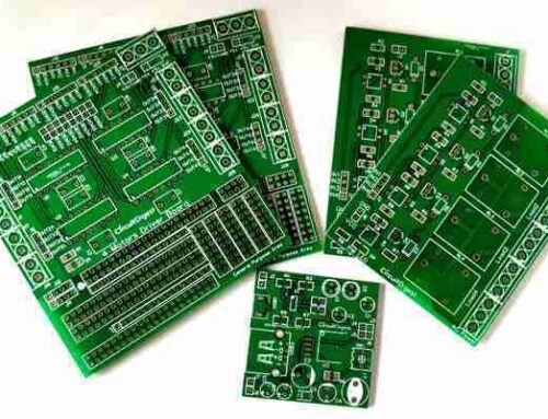
Table of Content
Contcat Us
Phone: +86-18123905375
Email: sales@circuitcardassembly.com
Skype: ali_youte
WhatsApp: +86-18123905375
Wechat: +86-18123905375

 Afrikaans
 Shqip
Shqip አማርኛ
አማርኛ العربية
 Հայերեն
 Azərbaycan dili
 Euskara
 Беларуская мова
 বাংলা
বাংলা Bosanski
 Български
 Català
 Cebuano
 Chichewa
 简体中文
简体中文 繁體中文
繁體中文 Corsu
Corsu Hrvatski
 Čeština
 Dansk
Dansk Nederlands
 Esperanto
 Eesti
Eesti Filipino
 Suomi
Suomi Français
 Frysk
Frysk Galego
 ქართული
 Deutsch
 Ελληνικά
 ગુજરાતી
 Kreyol ayisyen
 Harshen Hausa
 Ōlelo Hawaiʻi
 עִבְרִית
 हिन्दी
 Hmong
Hmong Magyar
 Íslenska
 Igbo
Igbo Bahasa Indonesia
 Gaeilge
 Italiano
 日本語
日本語 Basa Jawa
 ಕನ್ನಡ
ಕನ್ನಡ Қазақ тілі
 ភាសាខ្មែរ
 한국어
한국어 كوردی
كوردی Кыргызча
 ພາສາລາວ
 Latin
Latin Latviešu valoda
 Lietuvių kalba
 Lëtzebuergesch
 Македонски јазик
 Malagasy
 Bahasa Melayu
 മലയാളം
 Maltese
 Te Reo Māori
 मराठी
मराठी Монгол
 ဗမာစာ
ဗမာစာ नेपाली
 Norsk bokmål
 پښتو
پښتو فارسی
فارسی Polski
 Português
 ਪੰਜਾਬੀ
 Română
 Русский
 Samoan
 Gàidhlig
 Српски језик
 Sesotho
 Shona
Shona سنڌي
سنڌي සිංහල
සිංහල Slovenčina
 Slovenščina
 Afsoomaali
 Español
 Basa Sunda
 Kiswahili
 Svenska
 Тоҷикӣ
 தமிழ்
தமிழ் తెలుగు
 ไทย
ไทย Türkçe
 Українська
 اردو
اردو O‘zbekcha
 Tiếng Việt
 Cymraeg
 isiXhosa
 יידיש
יידיש Yorùbá
 Zulu
Zulu